Array substrate gate driving circuit, driving method thereof, and display device

A technology for gate drive circuits and array substrates, applied in static indicators, digital memory information, instruments, etc., can solve problems that are not conducive to the design of narrow borders of display panels, and achieve the effects of simple timing control and low circuit cost

Inactive Publication Date: 2019-08-02
BOE TECH GRP CO LTD +1
View PDF5 Cites 0 Cited by
  • Summary
  • Abstract
  • Description
  • Claims
  • Application Information

AI Technical Summary

Problems solved by technology

Therefore, the bezel will be increased to varying degrees (depending on the size of the additional transistor), which is not conducive to the realization of a narrow bezel design of the display panel

Method used


Image

  • Array substrate gate driving circuit, driving method thereof, and display device
  • Array substrate gate driving circuit, driving method thereof, and display device
  • Array substrate gate driving circuit, driving method thereof, and display device

Examples


Embodiment Construction

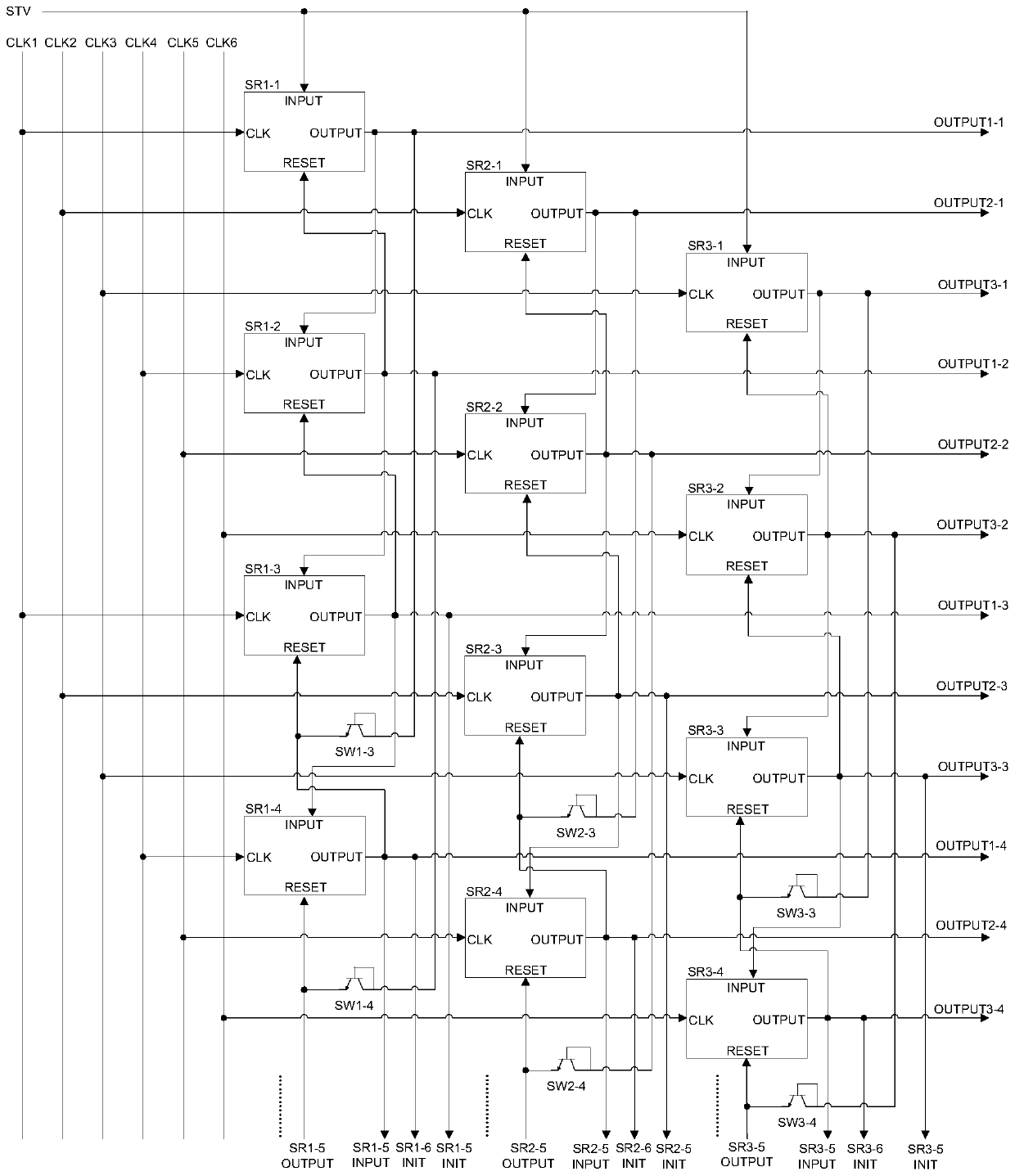
[0038] figure 1 The shown array substrate gate driving circuit includes at least one shift register group, and each shift register group includes a plurality of shift registers. In each shift register group, make the input end of the shift register located in the first stage receive the STV signal, and make the input ends of other stages of shift registers other than the first stage be connected to the one before the shift register. The output terminal of the shift register of the stage to receive the gate drive signal output from the shift register of the previous stage as the input signal, thereby cascading multiple shift registers in each shift register group together . For the convenience of expression, in this paper, "SRi-j" is used to represent the shift register cascaded at the jth level in the i-th shift register group, where the shift register SRi-j is located in the shift register SRi- The upper stage of (j+1), the shift register SRi-(j+1) is located in the lower s...


PUM


Abstract

Provided are an array substrate gate driving circuit, a driving method thereof, and a display device. The array substrate gate drive circuit includes at least one shift register group, each shift register group includes a plurality of shift registers cascaded together, the plurality of shift registers include a first shift register, and the connection position is at a second shift register after the first shift register and a third shift register connected after the second shift register, wherein the third shift register is provided with an initialization terminal, and the The initialization terminal is connected to the output terminal of the first shift register.

Description

technical field [0001] The present disclosure relates to an array substrate gate driving circuit, a driving method thereof, and a display device. Background technique [0002] The gate driver on array (Gate Driver on Array, GOA) technology integrates the gate driver circuit inside the display panel through a thin film transistor process, so as to reduce the cost of the gate driver circuit in the panel. Since there is no need for gate drive circuit bonding (Bonding), GOA technology can also increase the production capacity of the MDL process, and can realize the narrow frame design of the display panel. [0003] GOA circuits usually contain multiple shift registers cascaded. In order to prevent the abnormal display of the picture of the current frame from affecting the picture of the next frame, and at the same time, in order to prevent the black screen after booting, a Total Reset function can be added to the GOA circuit, that is, during the blanking period between two fram...

Claims


Application Information

Patent Timeline
Patent Type & Authority Patents(China)
IPC IPC(8): G09G3/20G11C19/28
CPCG09G3/20G11C19/28G09G2310/0267G09G2310/0286G09G2300/0408G09G3/2092
Inventor 白雅杰许卓张元波方琰邓鸣唐子杰金在光
Owner BOE TECH GRP CO LTD
Why Eureka
Try Eureka