

Solar silicon wafer surface defect detection device
A solar silicon wafer and defect detection technology, which is applied in semiconductor/solid-state device testing/measurement, electrical components, circuits, etc., can solve the problems of silicon wafer damage, large mechanical loss, and low long-term efficiency, so as to facilitate mechanical control and facilitate The effect of short control and operation process
- Summary
- Abstract
- Description
- Claims
- Application Information
AI Technical Summary
Benefits of technology
Problems solved by technology
Method used
Image


Examples
Embodiment 1
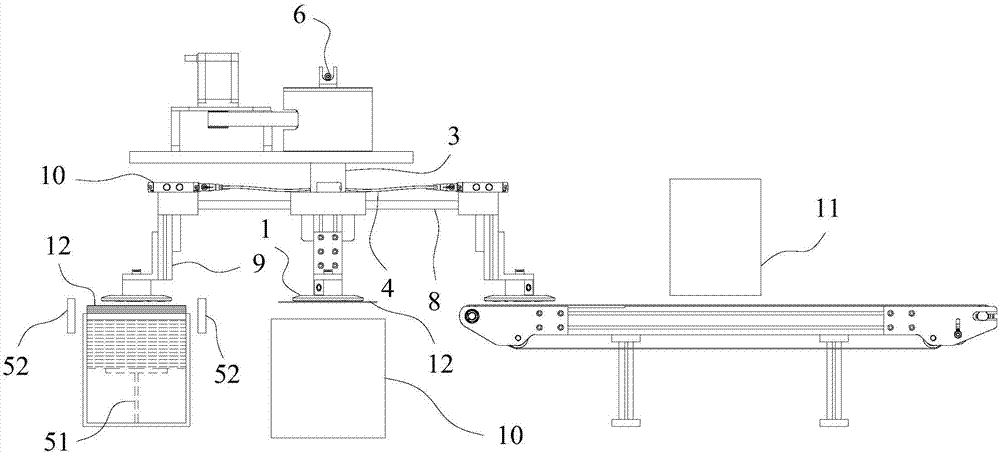
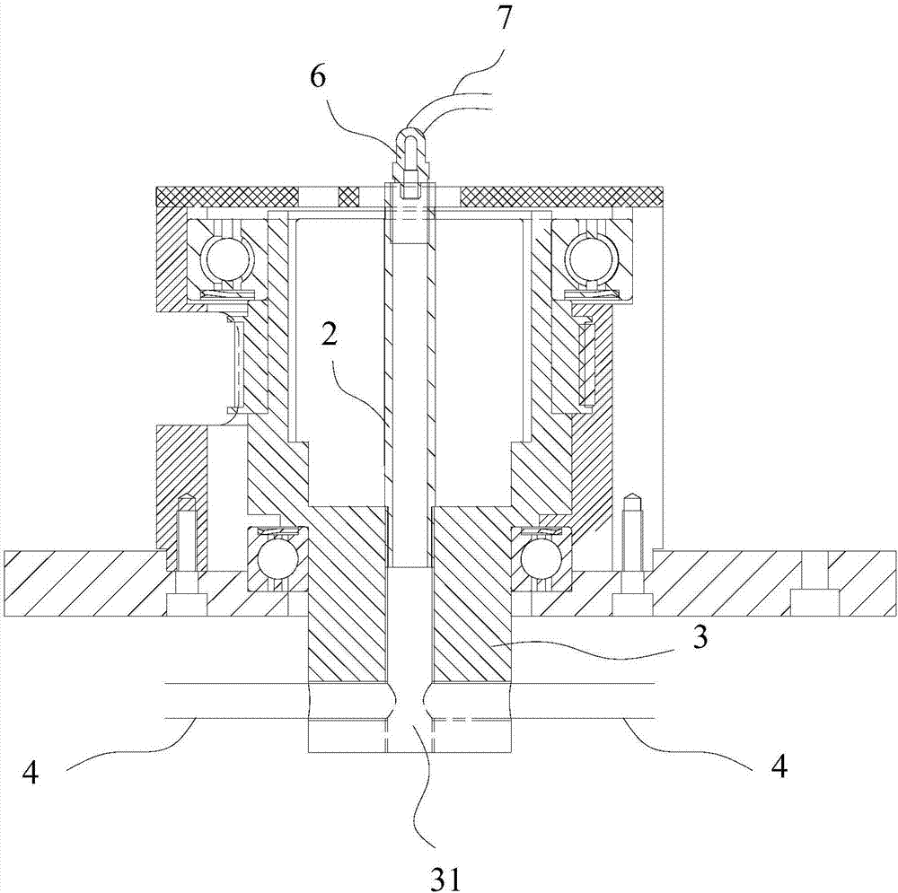
[0050] Such as Figure 1-3 , a surface defect detection device for solar silicon wafers according to the present invention, comprising a grabbing component, a circular track 8, a detection component, a gas distribution component, a display component, a feeding device, a feeding device, a drive system and a control system , the control system controls the driving system to drive the grabbing part, detection part, display part, feeding device and unloading device, the control system includes a processing module, and the grabbing part includes four suction cups 1, The gas distribution assembly includes an air guide tube 2 and a sleeve 3, the air guide tube 2 is a hollow copper tube, the sleeve 3 is provided with an inner hole 31, and the lower end of the air guide tube 2 is connected to the inner hole 31. The upper end of the air guide tube 2 is provided with an opening one, the opening one is connected to the air pipe two 7 through the rotary joint 6, the air pipe two 7 is conne...
PUM
 Abstract
Description
Claims
Application Information