Mold release film and method for manufacturing semiconductor package

A release film, semi-conductor technology, applied in semiconductor/solid-state device manufacturing, semiconductor devices, electric solid-state devices, etc., can solve the problem of destroying semiconductor components, etc., and achieve excellent anti-static effect and excellent transparency

Active Publication Date: 2017-08-01
ASAHI GLASS CO LTD
View PDF10 Cites 5 Cited by
  • Summary
  • Abstract
  • Description
  • Claims
  • Application Information

AI Technical Summary

Problems solved by technology

If the release film is easily charged, when the cured curable resin and the release film are peeled off, the release film is charged and then discharged, which may damage the semiconductor element

Method used


Image

  • Mold release film and method for manufacturing semiconductor package
  • Mold release film and method for manufacturing semiconductor package
  • Mold release film and method for manufacturing semiconductor package

Examples


no. 1 Embodiment approach

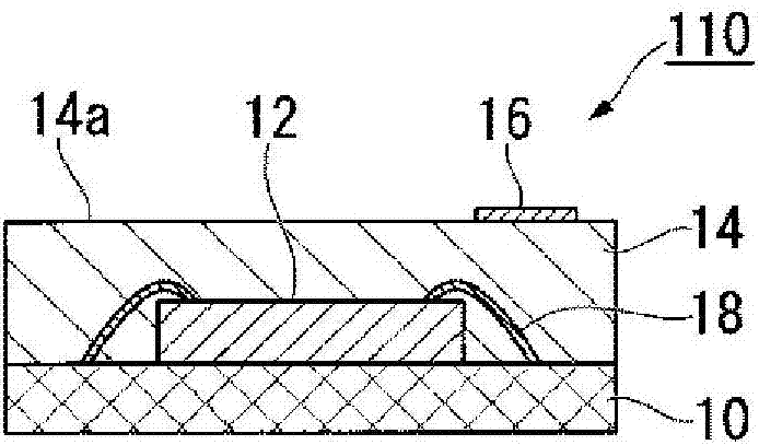
[0224] use Figure 5-7 The first embodiment of the manufacturing method of the semiconductor package of the present invention will be described. In this embodiment, the release film 1 is used as the release film and manufactured by compression molding. image 3 An example of a semiconductor package 110 is shown.

[0225] The manufacturing method of the semiconductor package according to this embodiment includes the following steps (α1) to (α7).

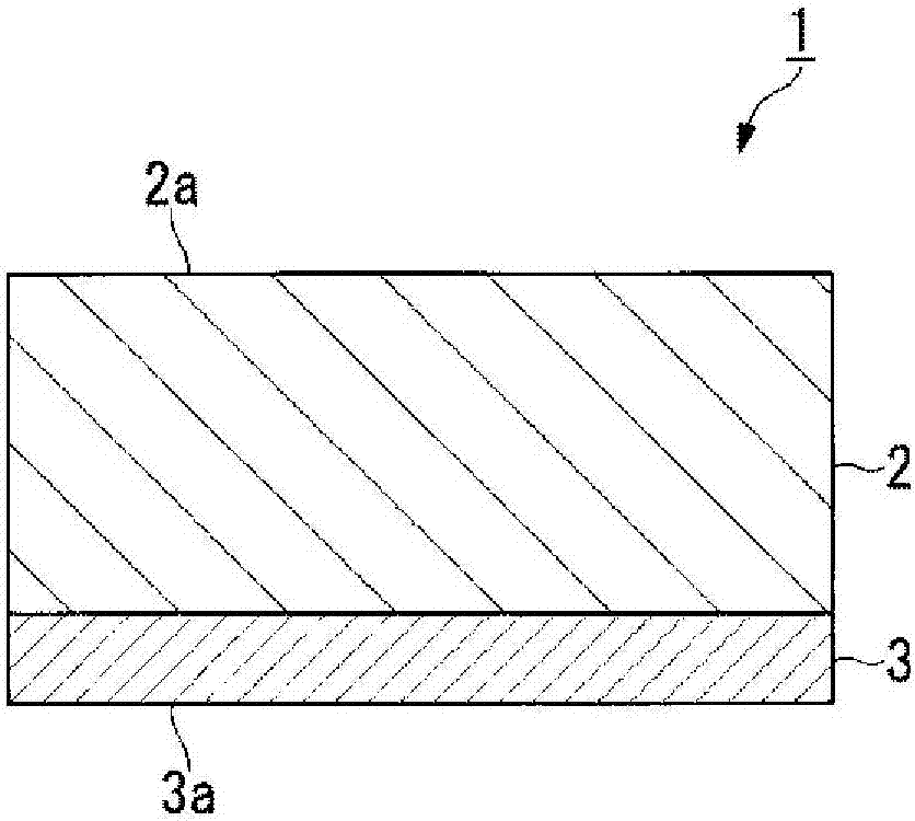
[0226] (α1) The mold release film 1 is arranged in a mold having a fixed upper mold 20, a cavity bottom surface member 22, and a frame-shaped movable lower mold 24 arranged around the periphery of the cavity bottom surface member 22, and the mold release film 1 covers all Describe the cavity 26 of the mould, and the surface 2a of the releasable substrate 2 side of the release film 1 faces the space in the cavity 26 (making the surface 3a on the antistatic layer 3 side contact the cavity surface of the mould) ( Figure 5 ).

[0227...

no. 2 Embodiment approach

[0234] use Figure 8-11 A second embodiment of the manufacturing method of the semiconductor package of the present invention will be described. In this embodiment, the release film 1 is used as the release film and manufactured by transfer molding. Figure 4 An example of a semiconductor package 120 is shown.

[0235] The manufacturing method of the semiconductor package according to this embodiment includes the following steps (β1) to (β5).

[0236] (β1) The release film 1 is arranged so that the release film 1 covers the cavity 54 of the upper die 50 of the mold having the upper die 50 and the lower die 52 and the surface 2a of the release film 1 on the release base 2 side faces Space in the cavity 54 (making the surface 3a on the antistatic layer 3 side contact with the cavity surface 56 of the upper mold 50) ( Figure 8 ).

[0237] (β2) The process of vacuum-adsorbing the release film 1 on the cavity surface 56 side of the upper mold 50 ( Figure 9 ).

[0238] (β3) ...

Embodiment

[0250] Examples are shown below to describe the present invention in detail. However, the present invention is not limited to the following description.

[0251] Among Examples 1 to 18 described later, Examples 1 to 13 are examples, and Examples 14 to 18 are comparative examples.

[0252] The evaluation methods and materials used in each example are shown below.

[0253] 〔Evaluation method〕

[0254] (thickness)

[0255] The thickness (μm) of the substrate was measured in accordance with ISO 4591:1992 (method B1 of JIS K7130:1999, measuring method of thickness of a sample collected from a plastic film or sheet by mass method).

[0256] The thickness (nm) of the antistatic layer was measured with a transmission type infrared film thickness meter RX-100 (manufactured by Kurabo Industries, Ltd. (Kurabo Industries, Ltd.)).

[0257] (arithmetic mean roughness Ra)

[0258] The arithmetic mean roughness Ra (μm) of the surface was measured in accordance with JIS B 0601:2013 (ISO 4...


PUM

PropertyMeasurementUnit
surface roughnessaaaaaaaaaa
thicknessaaaaaaaaaa
surface roughnessaaaaaaaaaa

Abstract

Provided are: a mold release film which exhibits excellent antistatic effect even in a high temperature environment, while having excellent transparency; and a method for manufacturing a semiconductor package, which uses this mold release film. A mold release film which is arranged on a mold surface that comes into contact with a curable resin during the production of a semiconductor package, wherein a semiconductor element is arranged within a mold and sealed with the curable resin, thereby forming a resin sealed part. This mold release film comprises: a mold releasing base 2 that comes into contact with the curable resin during the formation of the resin sealed part (said base containing no antistatic agent); and an antistatic layer 3 that comes into contact with the mold during the formation of the resin sealed part. The antistatic layer 3 contains at least one antistatic agent selected from the group consisting of conductive polymers and conductive metal oxides. This mold release film has a total light transmittance of 80% or more.

Description

technical field [0001] The present invention relates to a release film arranged on the cavity surface of a mold in the manufacture of a semiconductor package in which a semiconductor element is placed in a mold and sealed with a curable resin to form a resin sealing portion, and a semiconductor package using the release film Body manufacturing method. Background technique [0002] In order to block and protect the semiconductor element from outside air, it is usually sealed with a resin, and mounted on a substrate as a molded product called a package. The sealing of the semiconductor element is performed using a curable resin such as a thermosetting resin such as an epoxy resin. As a method of sealing a semiconductor element, for example, a method of arranging a substrate on which a semiconductor element is mounted so that the semiconductor element is located at a predetermined position in a cavity of a mold, filling the cavity with a curable resin, and curing it is known. ...

Claims


Application Information

Patent Timeline
Patent Type & Authority Applications(China)
IPC IPC(8): B29C33/62H01L21/56
CPCB29C33/62H01L21/56H01L2224/16227H01L2224/32225H01L2224/48091H01L2224/48227H01L2224/73204H01L2224/97H01L2924/18161H01L2224/85H01L2224/81H01L2924/00014H01L2224/16225H01L2924/00
Inventor 笠井涉铃木政己
Owner ASAHI GLASS CO LTD
Why Eureka
Try Eureka