Array substrate

An array substrate and sub-region technology, applied in nonlinear optics, instruments, optics, etc., can solve problems such as the decrease of liquid crystal panel transmittance

Active Publication Date: 2017-08-04
SHENZHEN CHINA STAR OPTOELECTRONICS SEMICON DISPLAY TECH CO LTD
View PDF7 Cites 36 Cited by
  • Summary
  • Abstract
  • Description
  • Claims
  • Application Information

AI Technical Summary

Problems solved by technology

[0004] This kind of rice-shaped slit electrode, because the angle between the strip branch in each pixel electrode area and the vertical trunk and the horizontal trunk is the same, there will be a certain visual color difference or visual color shift, and the transmittance of the liquid crystal panel will also drop

Method used


Image

  • Array substrate
  • Array substrate

Examples


Embodiment Construction

[0024] In order to further illustrate the technical means adopted by the present invention and its effects, the following describes in detail in conjunction with preferred embodiments of the present invention and accompanying drawings.

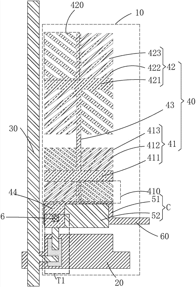
[0025] see figure 2 , the present invention provides an array substrate, comprising: a plurality of sub-pixels 10 arranged in an array, a plurality of horizontal scanning lines 20 arranged in parallel at intervals, and a plurality of vertical data lines 30 arranged in parallel at intervals;

[0026] Each row of sub-pixels 10 corresponds to a scanning line 20, and each column of sub-pixels 10 corresponds to a data line 30. Each sub-pixel 10 includes: a control thin film transistor T1 and a pixel electrode 40; the gate of the control thin film transistor T1 Electrically connected to the scan line 20 corresponding to the row of sub-pixels, the source is electrically connected to the data line 30 corresponding to the row of sub-pixels, and the dr...


PUM

PropertyMeasurementUnit
angleaaaaaaaaaa
angleaaaaaaaaaa
widthaaaaaaaaaa

Abstract

The invention provides an array substrate. Each sub-pixel in the array substrate comprises a control thin film transistor and a pixel electrode electrically connected with the control thin film transistor. Each pixel electrode comprises a main region pixel electrode, an auxiliary region pixel electrode and a first connecting electrode, wherein the main region pixel electrode and the auxiliary region pixel electrode are arranged in a spaced mode, and the first connecting electrode is electrically connected with the main region pixel electrode and the auxiliary region pixel electrode. The main region pixel electrodes and the auxiliary region pixel electrodes are slit electrodes shaped like a Chinese character 'mi'. The width of main region branch electrodes of the main region pixel electrodes is smaller than that of auxiliary region branch electrodes of the auxiliary region pixel electrodes, and the width of main region slits of the main region pixel electrodes is smaller than that of auxiliary region slits of the auxiliary region pixel electrodes. Color cast can be relieved through the structural difference of the main region pixel electrodes and the auxiliary region pixel electrodes, the number of TFTs in the sub-pixels is reduced, the opening rate of the pixels is increased, and the difficulty of optimal common voltage balance regulation and control of main regions and auxiliary regions is reduced.

Description

technical field [0001] The present invention relates to the field of display technology, in particular to an array substrate. Background technique [0002] A liquid crystal display (Liquid Crystal Display, LCD) is one of the most widely used flat panel displays at present, and a liquid crystal panel is a core component of the liquid crystal display. A liquid crystal panel is generally composed of a color filter substrate (ColorFilter, CF), a thin film transistor array substrate (Thin Film Transistor Array Substrate, TFTArray Substrate), and a liquid crystal layer (Liquid Crystal Layer) disposed between the two substrates. Generally, pixel electrodes and common electrodes are respectively arranged on the array substrate and the color filter substrate. When a voltage is applied to the pixel electrode and the common electrode, an electric field will be generated in the liquid crystal layer, which determines the orientation of the liquid crystal molecules, thereby adjusting the...

Claims


Application Information

Patent Timeline
Patent Type & Authority Applications(China)
IPC IPC(8): G02F1/1343G02F1/1368
CPCG02F1/134309G02F1/1368
Inventor 甘启明
Owner SHENZHEN CHINA STAR OPTOELECTRONICS SEMICON DISPLAY TECH CO LTD
Why Eureka
Try Eureka