

Pixel circuit, pixel driving method, and display device
A technology of pixel circuit and driving current, which is applied in the direction of static indicators, instruments, etc., can solve the problems of large driver chip area, low contrast of display panel, long gamma adjustment time, etc., and achieve the effect of avoiding false light emission
- Summary
- Abstract
- Description
- Claims
- Application Information
AI Technical Summary
Problems solved by technology
Method used
Image

Examples
Embodiment 1
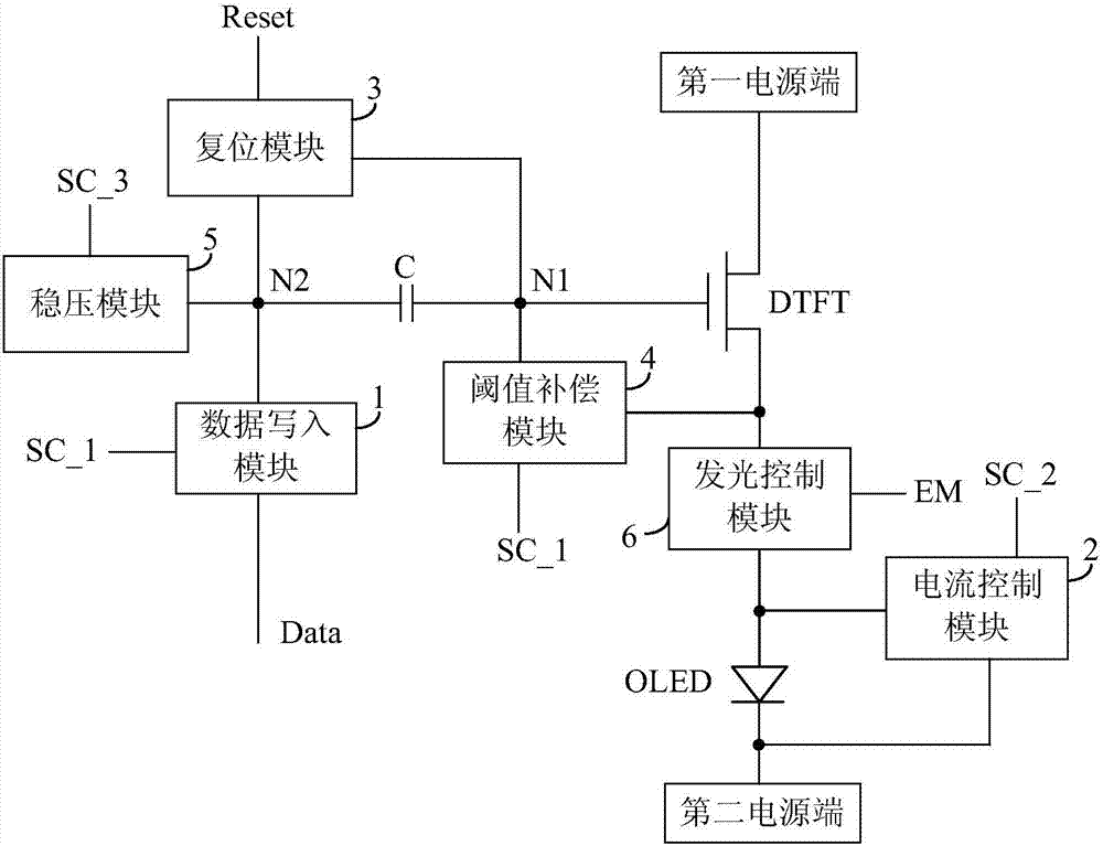
[0052] figure 1 A schematic circuit structure diagram of a pixel circuit provided in Embodiment 1 of the present invention, as shown in figure 1 As shown, the pixel circuit includes: a driving transistor DTFT, a capacitor C, a data writing module 1, a current control module 2 and a light emitting device OLED. The data writing module 1 is connected to the first end of the capacitor C, the second end of the capacitor C is connected to the control electrode of the driving transistor DTFT, the first electrode of the driving transistor DTFT is connected to the first power supply end, and the second electrode of the driving transistor DTFT It is connected with the first pole of the light emitting device OLED, the current control module 2 is connected with the first pole of the light emitting device OLED and the second power supply terminal, and the second pole of the light emitting device OLED is connected with the second power supply terminal.
[0053] The data writing module 1 is...
Embodiment 2
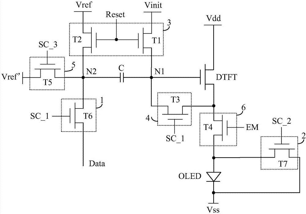
[0074] figure 2 A schematic circuit structure diagram of a pixel circuit provided in Embodiment 2 of the present invention, as shown in figure 2 As shown, the pixel circuit is an embodiment of the pixel circuit provided in the first embodiment above. Wherein, optionally, the reset module 3 includes: a first transistor T1 and a second transistor T2, the control pole of the first transistor T1 is connected to the reset control signal input line Reset, and the first pole of the first transistor T1 is connected to the third power terminal connected, the second pole of the first transistor T1 is connected to the second end of the capacitor C, the control pole of the second transistor T2 is connected to the reset control signal input line Reset, and the first pole of the second transistor T2 is connected to the fourth power supply terminal, The second pole of the second transistor T2 is connected to the first terminal of the capacitor C.
[0075] Optionally, the threshold compen...
Embodiment 3
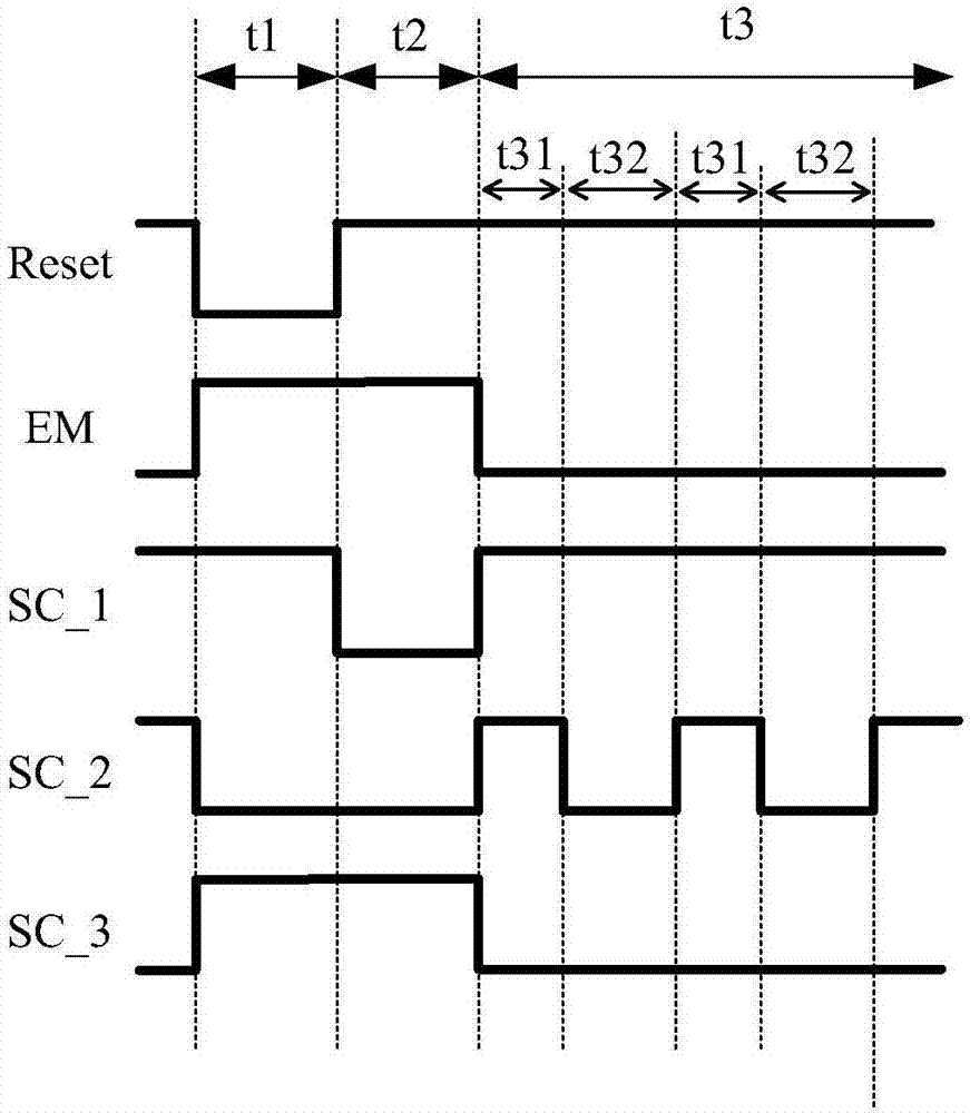
[0108] Figure 4 A flow chart of a pixel driving method provided by Embodiment 3 of the present invention, such as Figure 4 As shown, the pixel driving method is based on the pixel circuit, and the pixel circuit adopts the pixel circuit in the above-mentioned embodiment 1 or embodiment 2. The specific circuit structure can refer to the description in the above-mentioned embodiment 1 and embodiment 2, and will not be repeated here. . The pixel driving method includes:
[0109] Step S1 , in the data writing phase, the data writing module writes the data voltage provided by the data line into the first end of the capacitor under the control of the first control signal input from the first control signal input line.
[0110] Step S2, in the light-emitting stage, the driving transistor generates a driving current under the control of the voltage at the second terminal of the capacitor; the current control module controls the driving current to flow into the current under the con...
PUM
 Abstract
Description
Claims
Application Information