Fin field effect transistor and method of forming the same

A fin field effect and transistor technology, which is applied in semiconductor devices, semiconductor/solid state device manufacturing, electrical components, etc., can solve the problems that the performance of fin field effect transistors needs to be improved, and achieve the improvement of short channel effect and electric field control ability Enhanced, effective length-increased effect

Active Publication Date: 2019-12-03
SEMICON MFG INT (SHANGHAI) CORP +1
View PDF4 Cites 0 Cited by
  • Summary
  • Abstract
  • Description
  • Claims
  • Application Information

AI Technical Summary

Problems solved by technology

[0005] However, the performance of fin field effect transistors formed by existing technologies needs to be improved

Method used


Image

  • Fin field effect transistor and method of forming the same
  • Fin field effect transistor and method of forming the same
  • Fin field effect transistor and method of forming the same

Examples


no. 2 example

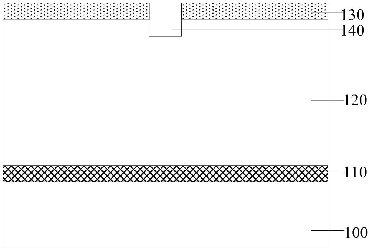
[0070] Figure 12 to Figure 20 It is a structural schematic diagram of the formation process of the fin field effect transistor in the second embodiment of the present invention.

[0071] The difference between the second embodiment and the first embodiment is that a groove is formed in the sacrificial layer, and the side wall of the groove has two pairs of groove protrusions, and each pair of groove protrusions is respectively located on both sides of the groove. side walls. The parts of the second embodiment that are the same as those of the first embodiment will not be described in detail.

[0072] refer to Figure 12 , Figure 12 for in Figure 6 Based on the schematic diagram formed, after forming the second protective layer 170, the second protective layer 170 and the sacrificial layer 120 are etched downward along the first groove 140 and the first opening 160, and the second protective layer 170 and the sacrificial layer 120 are formed at the bottom of the first op...

no. 3 example

[0103] Figure 21 to Figure 29 It is a structural schematic diagram of the formation process of the fin field effect transistor in the third embodiment of the present invention.

[0104] The difference between the third embodiment and the second embodiment is that a groove is formed in the sacrificial layer, and the side wall of the groove has three pairs of groove protrusions, and each pair of groove protrusions is respectively located on two sides of the groove. side walls. The parts of the third embodiment that are the same as those of the second embodiment will not be described in detail.

[0105] refer to Figure 21 , Figure 21 for in Figure 15 Based on the schematic diagram formed, after forming the fourth protective layer 230, the fourth protective layer 230 and the sacrificial layer 120 are etched downward along the first groove 140, the first opening 160, the second groove 200 and the second opening 220 , forming a third groove 340 at the bottom of the second o...


PUM


Abstract

The invention provides a fin field effect transistor and a formation method thereof. The method comprises the steps that a semiconductor substrate is provided, and an isolating layer is arranged on the semiconductor substrate; a sacrificial layer and a patterned mask layer are formed on the isolating layer from the bottom to the top in turn; the sacrificial layer is etched with the patterned mask layer acting as the mask until the surface of the isolating layer is exposed, grooves are formed in the sacrificial layer, multiple pairs of groove bulges are formed on the sidewall of the grooves, and each pair of groove bulges are arranged at the sidewall of the two sides of the grooves; fins fully filling in the grooves are formed, and fin bulges are formed in the groove bulges; and the sacrificial layer and the patterned mask layer are removed after the fins are formed. Electric field control capability reduction of the gate structure can be enhanced and the short channel effect can be improved by the method.

Description

technical field [0001] The invention relates to the field of semiconductor manufacturing, in particular to a fin field effect transistor and a forming method thereof. Background technique [0002] MOS transistors are one of the most important components in modern integrated circuits. The basic structure of a MOS transistor includes: a semiconductor substrate; a gate structure located on the surface of the semiconductor substrate, and source and drain regions located in the semiconductor substrate on both sides of the gate structure. The MOS transistor generates a switching signal by applying a voltage to the gate structure and adjusting the current through the channel at the bottom of the gate structure. [0003] With the development of semiconductor technology, the ability of the traditional planar MOS transistor to control the channel current becomes weaker, resulting in serious leakage current. Fin Field Effect Transistor (Fin FET) is an emerging multi-gate device, whic...

Claims


Application Information

Patent Timeline
Patent Type & Authority Patents(China)
IPC IPC(8): H01L29/78H01L21/336
CPCH01L29/66795H01L29/785
Inventor 王彦韩秋华张海洋
Owner SEMICON MFG INT (SHANGHAI) CORP
Why Eureka
Try Eureka