

Fin field effect transistor and formation method thereof
A fin field effect and transistor technology, which is applied in semiconductor devices, semiconductor/solid state device manufacturing, electrical components, etc., can solve the problems that the performance of fin field effect transistors needs to be improved, and achieve the improvement of short channel effect and electric field control ability Enhanced, effective length-increased effects
- Summary
- Abstract
- Description
- Claims
- Application Information
AI Technical Summary
Problems solved by technology
Method used
Image

Examples
no. 1 example
[0031] Figure 1 to Figure 7 It is a structural schematic diagram of the formation process of the fin field effect transistor in the first embodiment of the present invention.
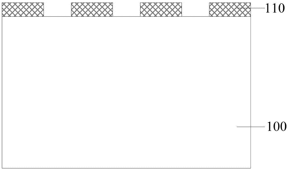
[0032] refer to figure 1 , providing a semiconductor substrate 100 .
[0033] In this embodiment, the material of the semiconductor substrate 100 is single crystal silicon.
[0034] It should be noted that, since a part of the semiconductor substrate 100 will form a fin in the subsequent process, the material of the fin must be a single crystal material, so the material of the semiconductor substrate 100 needs to be a single crystal silicon material.
[0035] In this embodiment, the crystal orientation of the surface of the semiconductor substrate 100 is . In other embodiments, the surface of the semiconductor substrate 100 may also choose other crystal orientations, such as , , or , and so on.
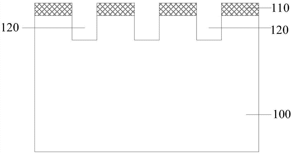
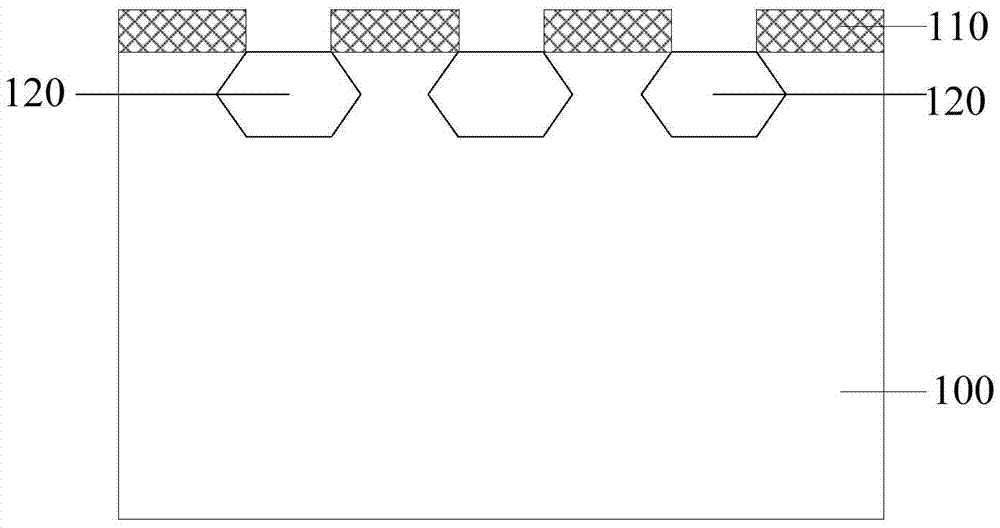
[0036] continue to refer figure 1 , forming a patterned mask layer 110 on the semiconductor substrat...
no. 2 example
[0071]The difference between the second embodiment and the first embodiment is that a trench is formed in the semiconductor substrate, and two corresponding pairs of trench depressions are formed on the sidewalls on both sides of the trench, each pair of trench depressions is respectively located in the trench The sidewalls on both sides of the groove, the semiconductor substrate between the adjacent grooves are used as fins, and the regions of the pair of recesses in the grooves form the pair of fin protrusions. The parts of the second embodiment that are the same as those of the first embodiment will not be described in detail again.
[0072] Figure 8 to Figure 11 It is a structural schematic diagram of the formation process of the fin field effect transistor in the second embodiment of the present invention.
[0073] refer to Figure 8 , Figure 8 for in Figure 6 Based on the schematic diagram formed, after the second wet etching, a second protection layer 260 is form...
no. 3 example
[0095] The difference between the third embodiment and the second embodiment is that a trench is formed in the semiconductor substrate, and three corresponding pairs of trench depressions are formed on the sidewalls of the two sides of the trench, and each pair of trench depressions is respectively located at The sidewalls on both sides of the grooves, the semiconductor substrate between the adjacent grooves serve as fins, and the regions of the pairs of recesses in the grooves form the pairs of fins and protrusions. The parts of the third embodiment that are the same as those of the second embodiment will not be described in detail.
[0096] Figure 12 to Figure 15 It is a structural schematic diagram of the formation process of the fin field effect transistor in the third embodiment of the present invention.
[0097] refer to Figure 12 , Figure 12 for in Figure 10 Based on the schematic diagram formed, after the third wet etching, a third protective layer 390 is forme...
PUM
 Abstract
Description
Claims
Application Information