Pixel structure

A pixel structure, strip-shaped technology, applied in semiconductor devices, electrical components, circuits, etc., can solve the problems affecting the electrical properties of thin film transistors, hump and other issues, and achieve the effect of improving electric field control ability, modifying edge current, and improving hump phenomenon.

Active Publication Date: 2017-06-27
AU OPTRONICS CORP
View PDF4 Cites 2 Cited by
  • Summary
  • Abstract
  • Description
  • Claims
  • Application Information

AI Technical Summary

Problems solved by technology

However, due to the influence of process factors, the current characteristics near the edge of the TFT channel may be different from that in the middle of the channel, so that the transfer characteristics at the edge of the TFT will be triggered in advance, resulting in a hump phenomenon in the critical region, which will affect the TFT performance. electrical

Method used


Image

  • Pixel structure
  • Pixel structure
  • Pixel structure

Examples


Embodiment Construction

[0065] A number of embodiments of the present invention will be disclosed in the following figures. For the sake of clarity, many practical details will be described together in the following description. It should be understood, however, that these practical details should not be used to limit the invention. That is, in some embodiments of the present invention, these practical details are unnecessary. In addition, for the sake of simplifying the drawings, some well-known structures and components will be shown in a simple and schematic manner in the drawings.

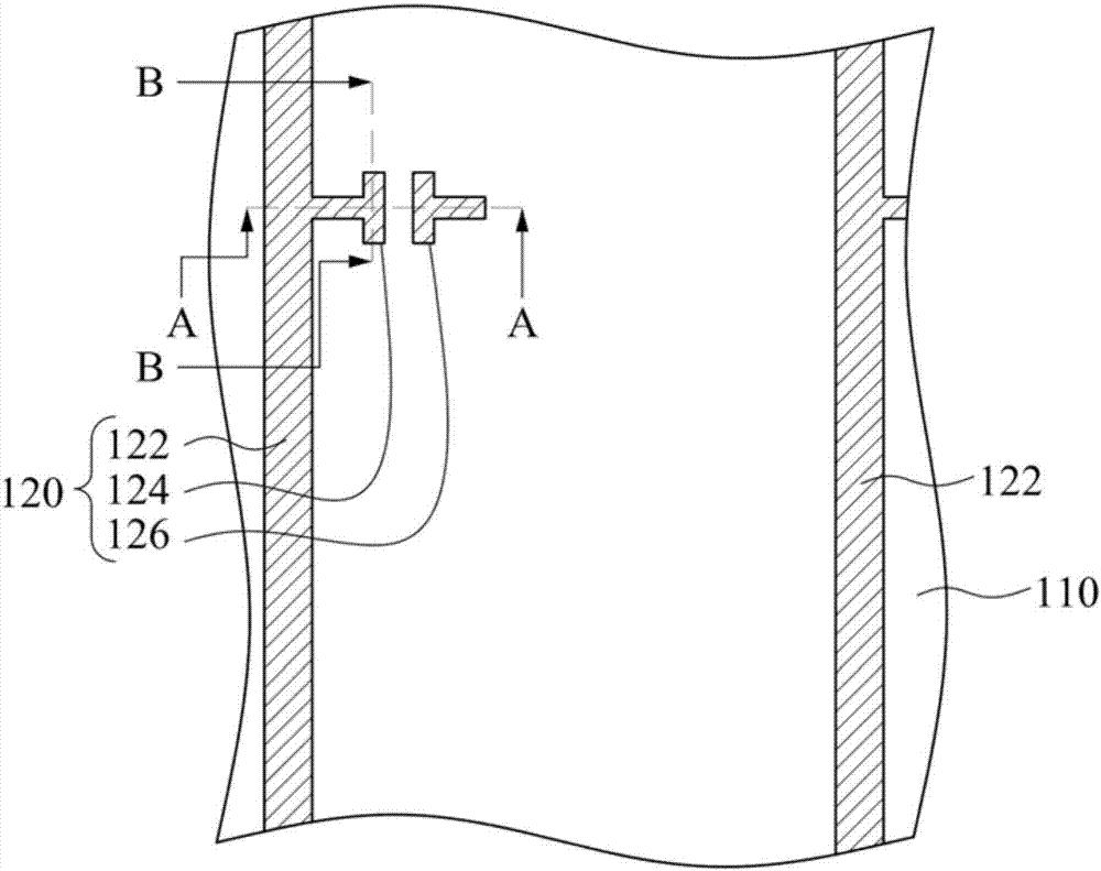
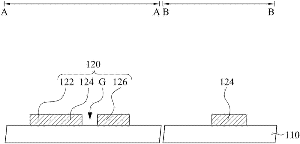
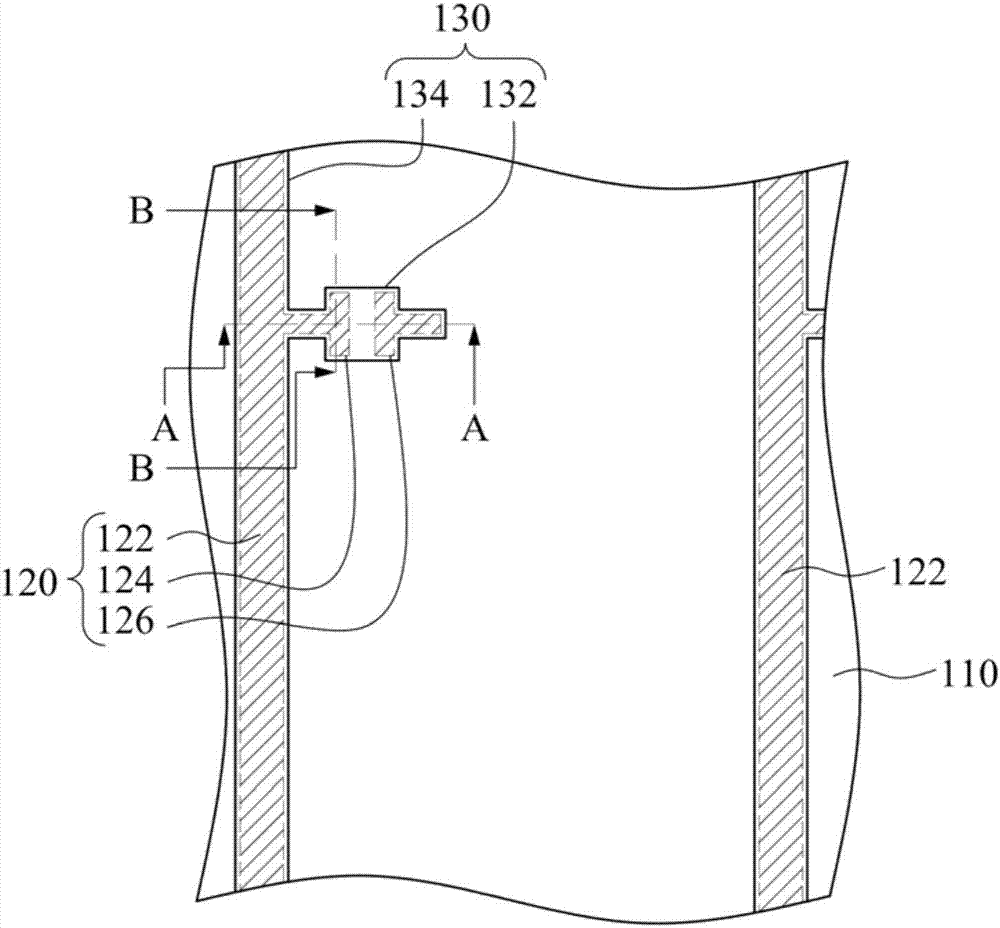
[0066] Figure 1A to Figure 4A It is a top view of each stage of the manufacturing method of the pixel structure 100 in the first embodiment of the present invention, and Figure 1B to Figure 4B respectively Figure 1A to Figure 4A Sectional view along line segments A-A and B-B. Please refer to Figure 1A and Figure 1B . A substrate 110 is provided. The material of the substrate 110 can be glass, quartz, organi...


PUM


Abstract

The present invention discloses a pixel structure including a data line, a gate line, an active element, a second organic semiconductor layer and a pixel electrode. The gate lines are interleaved with the data lines. The active element electrically connects the data line to the gate line. The active element comprises a source, a drain, a first organic semiconductor layer and a gate. The source is electrically connected to the data line. The organic semiconductor layer covers the source and drain. The organic semiconductor layer has a channel width direction between the source and the drain. The gate electrode is provided on the organic semiconductor layer and electrically connected to the gate line. The gate protrudes from the organic semiconductor layer in the channel width direction. The second organic semiconductor layer covers the data lines and is connected to the organic semiconductor layer. The pixel electrode is electrically connected to the drain.

Description

technical field [0001] The present invention relates to a pixel structure, in particular to a pixel structure of an organic display device. Background technique [0002] With the advancement of process technology, various types of display applications are constantly being introduced. In response to the requirements of light, thin, short, small and portable display applications, the next generation of display applications is developing towards the trend of easy portability. Thin film transistors are widely used in displays, and their structural design or material selection will directly affect the performance of the product. [0003] Generally speaking, a thin film transistor has at least a gate, a source, a drain, and a channel layer. The conductivity of the channel layer can be changed by controlling the voltage of the gate, so that a conduction is formed between the source and the drain. state of pass (open) or insulate (close). However, due to the influence of process ...

Claims


Application Information

Patent Timeline
IPC IPC(8): H01L27/12H01L29/423
CPCH01L27/124H01L29/42356H01L29/42384
Inventor 陈维翰刘冠显蔡佳宏吴安茹许世华涂峻豪刘竹育
Owner AU OPTRONICS CORP
Why Eureka
Try Eureka