Circuit board and method for producing circuit board

Pending Publication Date: 2022-06-16
IDEMITSU KOSAN CO LTD
View PDF0 Cites 0 Cited by
  • Summary
  • Abstract
  • Description
  • Claims
  • Application Information

AI Technical Summary

Benefits of technology

[0114]The inorganic material is added, for example, for the purpose of improving mechanical properties such as strength, surface hardness, dimensional stability, or the like, or increasing electrical properties such as conductivity. Specific examples of the inorganic material include, for example, silica (silicon dioxide), titania (titanium dioxide), alumina (aluminum oxide), Sn-containing In2O3 (ITO), Zn-containing In2O3, a co-substituted compound of In2O3 (an oxide in which tetravalent element and divalent element are substituted with trivalent In), Sb-containing SnO2 (ATO), ZnO, Al-containing ZnO (AZO), Ga-containing ZnO (GZO), and the like.
[0115]The curing agent is added, for example, for the purpose of improving mechanical properties such as strength, surface hardness, dimensional stability, or the like. Specific examples of the curing agent include, for example, a thermosetting agent such as a phenol resin, and a photocuring agent based on an acrylate-based monomer and a photopolymerizable initiator.
[0116]The plasticizer is added, for example, for the purpose of

Problems solved by technology

However, since a resin substrate having such a low dielectric loss tangent has low adhesiveness with adhesives, the necessity of strengthening the anchor effect by roughening the surface of the metal layer becomes greater.
On the other hand, the higher the frequency of electrical signals is, the more the current concentrates on the surface of the conductor (skin

Method used


Image

  • Circuit board and method for producing circuit board
  • Circuit board and method for producing circuit board
  • Circuit board and method for producing circuit board

Examples


production example 1

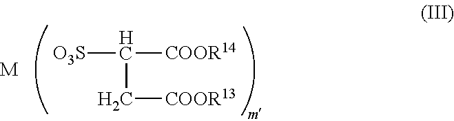
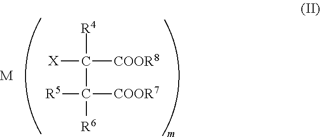
[Production of the Polyaniline Complex]

[0159]A solution obtained by dissolving 37.8 g of “Aerosol OT” (sodium di-2-ethylhexylsulfosuccinate) (AOT) and 1.47 g of “Sorbon T-20” (manufactured by Toho Chemical Industry Co., Ltd.) as a nonionic emulsifier having a polyoxyethylene sorbitan fatty acid ester structure in 600 mL of toluene was put in a 6 L separable flask placed under a steam of nitrogen, and 22.2 g of aniline was further added to this solution. Thereafter, 1800 mL of 1 M phosphoric acid was added to the solution, and the temperature of the solution having two liquid phases of toluene and water was cooled to 5° C.

[0160]When the internal temperature of the solution reached 5° C., the solution was stirred at 390 revolutions per minute. A solution of 65.7 g of ammonium persulfate dissolved in 600 mL of 1 M phosphoric acid was added dropwise over a period of 2 hours using a dropping funnel. The reaction was carried out for 18 hours from the start of the dropwise addition, while ...

example 1

Preparation of Coating Liquid 1

[0163]27 g of propylene glycol monobutyl ether, 53 g of anone, and 9 g of toluene were mixed to prepare a mixed solvent. 1.2 g of polyester resin (“Vylon GK810” manufactured by TOYOBO CO., LTD.), 6 g of polyester urethane resin (“Vylon UR1350” manufactured by TOYOBO CO., LTD.), and 1 g of a curing agent (“JA-980” manufactured by JUJO CHEMICAL CO., LTD.) were dissolved in the mixed solvent. To the solution, 2.7 g of the polyaniline complex obtained in Production Example 1 was dissolved. A resin modifier (“VD-3” manufactured by SHIKOKU CHEMICALS CORPORATION) was dispersed to the solution to obtain a coating liquid 1. The concentration of the polyaniline complex in the total solid content in the coating liquid 1 was 39%.

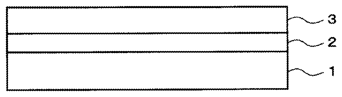
[Production and Evaluation of the Circuit Substrate]

(Active Energy Ray Irradiation Step)

[0164]With the use of an ultraviolet irradiation apparatus (“Conveyor UV irradiation apparatus” manufactured by GS Yuasa Corporation, a light source: m...

example 2

[0178]The circuit substrate was manufactured and evaluated in the same manner as in Example 1 except that a polyimide film (Kapton EN manufactured by DU PONT-TORAY CO., LTD., dielectric loss tangent: 0.0126 (10 GHz)) was used as the base material instead of the SPS resin film. The results are shown in Table 1.


PUM

PropertyMeasurementUnit
Lengthaaaaaaaaaa
Percent by massaaaaaaaaaa
Thicknessaaaaaaaaaa

Abstract

A circuit substrate comprising, in the following stacked order, a resin base material 1 having a dielectric loss tangent of 0.015 or lower, a polyaniline layer 2 comprising a substituted or unsubstituted polyaniline, and a metal layer 3, wherein the metal layer 3 has a surface roughness RzJIS of 0.5 μm or less at the surface on the side of the polyaniline layer 2.

Description

TECHNICAL FIELD[0001]The invention relates to a circuit substrate and a method of manufacturing a circuit substrate.BACKGROUND ART[0002]Recently, the utilization of high-frequency electrical signals has become active in a wide variety of fields including, for example, in-vehicle radar and next-generation mobile phones, etc., and circuit substrates suitable for transmission of high-frequency electrical signals are required.[0003]As a conventional circuit substrate, for example, one in which a base material and a metal layer (copper foil or the like) are bonded together by an adhesive is used as disclosed in Patent Document 1.RELATED ART DOCUMENTSPatent Documents[0004][Patent Document 1] JP H5-226831 ASUMMARY OF THE INVENTION[0005]When a base material and a metal layer are adhered to each other by an adhesive to form a circuit substrate as in the prior art, a method such as an etching treatment is usually employed, which gives to the surface of the metal layer unevenness (for example,...

Claims


Application Information

Patent Timeline
IPC IPC(8): H05K3/38H05K1/03H05K1/02C23C18/20C23C18/30C23C18/40
CPCH05K3/387H05K1/036H05K1/0242C23C18/204C23C18/30H05K1/09H05K2201/0154H05K2201/0141H05K2201/015H05K2201/0158C23C18/40C08J7/00C23C18/208C23C18/38H05K2201/0195H05K2203/072H05K3/022H05K2201/0329H05K2203/0716
Inventor FUKATSU, FUMIOKIHACHIYA, SATOSHI
Owner IDEMITSU KOSAN CO LTD
Why Eureka
Try Eureka