
Method for producing a single crystal from semiconductor material by the fz method; device for carrying out the method and semiconductor silicon wafer

Pending Publication Date: 2021-07-22
SILTRONIC AG
View PDF0 Cites 0 Cited by
  • Summary
  • Abstract
  • Description
  • Claims
  • Application Information

AI Technical Summary

Benefits of technology

The invention describes a process for growing single crystals of semiconductor material that are doped with a dopant. The process involves creating a molten zone between a feed rod and a growing single crystal, melting the feed rod material in a high frequency magnetic field, and crystallizing the molten material onto the growing single crystal while rotating it. An alternating magnetic field is then applied to the molten zone, which is not axisymmetric with respect to the axis of rotation of the growing single crystal. The technical effect of this invention is to provide a more efficient and precise method for growing high-quality semiconductor single crystals.

Problems solved by technology

Due to, among other things, the comparatively small segregation coefficients of n-type dopants such as phosphorus, arsenic and antimony, it is more difficult to achieve a homogenous distribution of such a dopant in the growing single crystal.

Method used


Image

  • Method for producing a single crystal from semiconductor material by the fz method; device for carrying out the method and semiconductor silicon wafer
  • Method for producing a single crystal from semiconductor material by the fz method; device for carrying out the method and semiconductor silicon wafer
  • Method for producing a single crystal from semiconductor material by the fz method; device for carrying out the method and semiconductor silicon wafer

Examples


Embodiment Construction

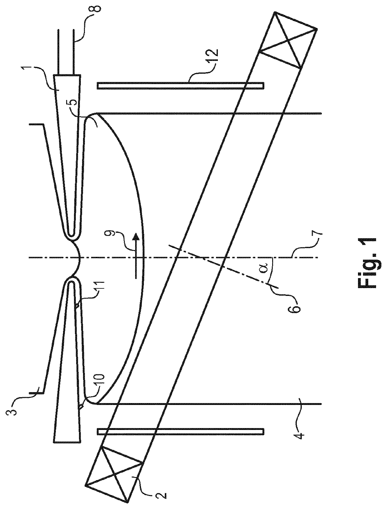
[0018]The inventors have found that it is advantageous to arrange the second induction coil, which imposes the alternating magnetic field on the molten zone, tilted from a horizontal position in order to solve the task. The axis through the center of the second induction coil and the axis of rotation of the growing single crystal include an angle different from zero. This angle is preferably not less than 15° and not more than 30°. The alternating magnetic field exerts an electromagnetic force on the molten zone, which improves the mixing of dopant in the molten zone and aligns the flow in the center of the molten zone markedly asymmetrically. This ensures that the dopant is more uniformly incorporated, especially in the center of the growing single crystal.

[0019]The process is effective independent of the dopant type. It can therefore be used to produce single crystals of semiconductor material doped with n-type dopant as well as those doped with p-type dopant. It is particularly a...


PUM


Abstract

Single crystals of semiconductor material are produced by an FZ method, wherein a molten zone is created between a feed rod and a growing single crystal; the method involvingmelting feed rod material in a high frequency magnetic field of a first induction coil;crystallizing material of the molten zone on top of the growing single crystal;rotating the growing single crystal about an axis of rotation and changing the direction of rotation and the speed of rotation according to a predetermined pattern; andimposing an alternating magnetic field of a second induction coil on the molten zone, wherein the alternating magnetic field is not axisymmetric with respect to the axis of rotation of the growing single crystal.

Description

CROSS REFERENCE TO RELATED APPLICATIONS[0001]This application is the U.S. National Phase of PCT Appln. No. PCT / EP2019 / 064554 filed Jun. 4, 2019, which claims priority to German Application No. 10 2018 210 317.8 filed Jun. 25, 2018, the disclosures of which are incorporated in their entirety by reference herein.BACKGROUND OF THE INVENTIONField of the Invention[0002]The object of the invention is a process for producing a single crystal of semiconductor material according to the FZ method, comprising creating a melting zone between a feed rod and a growing single crystal. The invention also concerns a device suitable for carrying out the process and a silicon semiconductor wafer doped with n-type dopant which becomes accessible by the process.2. DESCRIPTION OF THE RELATED ART[0003]The floating zone method comprises creating a molten zone between a feed rod and a growing single crystal, melting material of the feed rod in a high frequency magnetic field, and crystallizing material of t...

Claims


Application Information

Patent Timeline
IPC IPC(8): C30B13/20C30B29/06C30B30/04C30B13/12H01L21/02H01L29/16H01L29/36
CPCC30B13/20C30B29/06C30B30/04C30B13/12H01L29/36H01L21/02576H01L21/02625H01L29/16H01L21/02532C30B13/26
Inventor ALTMANNSHOFER, LUDWIGMEISTERERNST, GOETZRATNIEKS, GUNDARSZITZELSBERGER, SIMON
Owner SILTRONIC AG
Learn More