Semiconductor structure and forming method thereof

A semiconductor and isolation structure technology, applied in the field of semiconductor structure and its formation, can solve problems such as poor device performance, achieve the effect of improving electrical performance and increasing breakdown voltage

Pending Publication Date: 2020-02-28
SEMICON MFG INT (SHANGHAI) CORP +1
View PDF0 Cites 0 Cited by
  • Summary
  • Abstract
  • Description
  • Claims
  • Application Information

AI Technical Summary

Problems solved by technology

[0005] However, after introducing the single-diffusion block isolation structure in the semiconductor structure, the device still has the problem of poor performance

Method used


Image

  • Semiconductor structure and forming method thereof
  • Semiconductor structure and forming method thereof
  • Semiconductor structure and forming method thereof

Examples


Embodiment Construction

[0018] It can be seen from the background art that after introducing a single-diffusion isolation structure into a semiconductor structure, the device still has the problem of poor performance. The reason why its performance needs to be improved is analyzed in conjunction with a semiconductor structure.

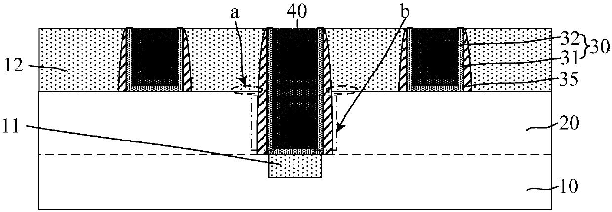
[0019] refer to figure 1 , shows a schematic structural view of a semiconductor structure.

[0020] The semiconductor structure includes: a base (not marked), including a substrate 10 and a plurality of discrete fins 20 located on the substrate 10, the extending direction of the fins 20 being a first direction (not marked), The direction parallel to the surface of the substrate 10 and perpendicular to the first direction is the second direction (not marked), and the fins 20 are arranged in a matrix in the first direction and the second direction; the isolation structure (not marked) marked), located on the substrate 10 exposed by the fins 20, the isolation structure include...


PUM


Abstract

The invention provides a semiconductor structure and a forming method thereof. The forming method comprises the steps: forming a base including a substrate and a plurality of discrete fin parts positioned on the substrate; and forming a metal grid structure across the fin parts, wherein the metal grid structure covers part of the top and part of the side walls of the fin parts; forming an isolation grid structure on the substrate between the adjacent fin parts along the extension direction of the fin parts, wherein the material of the isolation grid structure is a dielectric material. The isolation grid structure is formed on the substrate between the adjacent fin parts, and the material of the isolation grid structure is the dielectric material; in the semiconductor process, the isolationgrid structure is usually formed in the same process step as the metal grid structure across the fin parts, i.e., the material of the isolation grid structure usually includes the metal material. Thedielectric material is selected as the material of the isolation grid structure so that the isolation grid structure has insulation characteristics, electrical connection between the isolation grid structure and the adjacent fin parts is avoided, and thus the breakdown voltage of the isolation grid structure can be improved and the electrical performance of the device can be improved.

Description

technical field [0001] The invention relates to the field of semiconductor manufacturing, in particular to a semiconductor structure and a forming method thereof. Background technique [0002] With the rapid development of semiconductor manufacturing technology, semiconductor devices are developing towards higher component density and higher integration. Transistors are currently being widely used as one of the basic semiconductor devices. Therefore, with the increase in the density and integration of semiconductor devices, the gate size of planar transistors is getting shorter and shorter. The control ability of traditional planar transistors on the channel current becomes weaker, and the short channel effect occurs, causing the leakage current to increase. affect the electrical performance of semiconductor devices. [0003] In order to better adapt to the reduction of feature size, the semiconductor process has gradually begun to transition from planar MOSFETs to three-d...

Claims


Application Information

Patent Timeline
IPC IPC(8): H01L29/78H01L21/336H01L29/06H01L29/423
CPCH01L29/785H01L29/66795H01L29/0684H01L29/42356
Inventor 冯军宏
Owner SEMICON MFG INT (SHANGHAI) CORP
Why Eureka
Try Eureka