Fin field effect transistor and method of forming the same

A fin field effect and transistor technology, which is applied in semiconductor devices, semiconductor/solid state device manufacturing, electrical components, etc., can solve the problems that the performance of fin field effect transistors needs to be improved, and achieve the reduction of short channel effect and electric field control ability Enhanced, effective length-increased effects

Active Publication Date: 2019-11-01
SEMICON MFG INT (SHANGHAI) CORP +1
View PDF4 Cites 0 Cited by
  • Summary
  • Abstract
  • Description
  • Claims
  • Application Information

AI Technical Summary

Problems solved by technology

[0005] However, the performance of fin field effect transistors formed by existing technologies needs to be improved

Method used


Image

  • Fin field effect transistor and method of forming the same
  • Fin field effect transistor and method of forming the same
  • Fin field effect transistor and method of forming the same

Examples


Embodiment Construction

[0024] For the analysis of the fin field effect transistor formed in the prior art, the fin portion of the fin field effect transistor is usually formed by patterning the semiconductor substrate, and the sidewall of the fin portion is planar. With the further increase of the feature size, especially when the technology node is reduced below 10nm, the short channel effect of the fin field effect transistor in the prior art is serious.

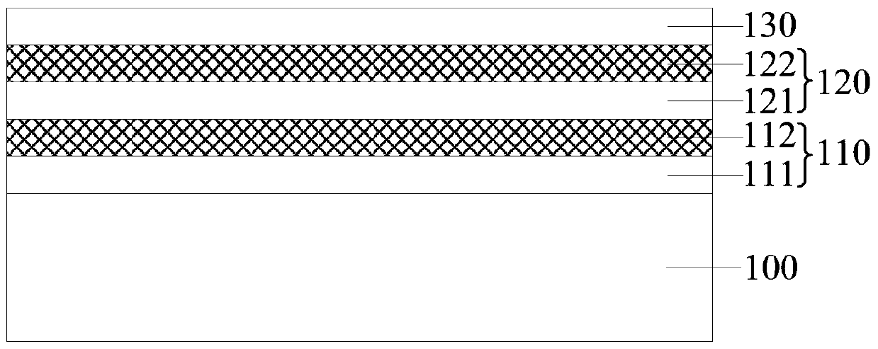
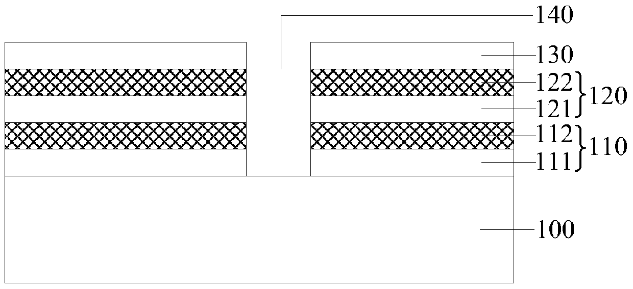
[0025] On this basis, the present invention provides a method for forming a fin field effect transistor, in which several layers of sacrificial unit layers are sequentially formed on the semiconductor substrate from bottom to top, and the sacrificial unit layers include the bottom sacrificial layer and the The top sacrificial layer on the bottom sacrificial layer, and then a protective layer is formed on the several sacrificial unit layers; an anisotropic dry etching process is used to etch the protective layer and the sacrificial unit layer unti...


PUM


Abstract

A fin field effect transistor and its forming method, wherein the method includes: providing a semiconductor substrate; sequentially forming several sacrificial unit layers on the semiconductor substrate from bottom to top, the sacrificial unit layer includes a bottom sacrificial layer and a bottom sacrificial layer The top sacrificial layer on top; a protective layer is formed on several sacrificial unit layers, and the material of the protective layer is the same as that of the bottom sacrificial layer; an anisotropic dry etching process is used to etch the protective layer and the sacrificial unit layer until the semiconductor is exposed On the surface of the substrate, a groove is formed that runs through the thickness of the protective layer and the sacrificial unit layer; the sacrificial unit layer and the protective layer on the sidewall of the trench are wet etched, and the etching rate of the top layer sacrificial layer is greater than that of the wet etching. The etch rate of the bottom sacrificial layer; fill the fins in the trenches after wet etching, so that the side walls of the fins have protrusions, and then remove the protective layer and the sacrificial unit layer. The method can enhance the electric field control capability of the grid structure and further improve the short channel effect.

Description

technical field [0001] The invention relates to the field of semiconductor manufacturing, in particular to a fin field effect transistor and a forming method thereof. Background technique [0002] MOS transistors are one of the most important components in modern integrated circuits. The basic structure of a MOS transistor includes: a semiconductor substrate; a gate structure located on the surface of the semiconductor substrate, and source and drain regions located in the semiconductor substrate on both sides of the gate structure. The MOS transistor generates a switching signal by applying a voltage to the gate structure and adjusting the current through the channel at the bottom of the gate structure. [0003] With the development of semiconductor technology, the ability of the traditional planar MOS transistor to control the channel current becomes weaker, resulting in serious leakage current. Fin Field Effect Transistor (Fin FET) is an emerging multi-gate device, whic...

Claims


Application Information

Patent Timeline
Patent Type & Authority Patents(China)
IPC IPC(8): H01L29/10H01L21/336H01L29/78
CPCH01L29/1033H01L29/66795H01L29/785H01L29/7853
Inventor 黄敬勇王彦
Owner SEMICON MFG INT (SHANGHAI) CORP
Why Eureka
Try Eureka