Power semiconductor chip, photolithography mask thereof and exposure method of power semiconductor chip
A technology for power semiconductors and exposure methods, which is applied to microlithography exposure equipment, photolithography process exposure devices, and pattern surface photolithography processes, etc. Key dimensions and other issues to achieve the effect of reducing the number of chips, reducing the number, and improving the error
- Summary
- Abstract
- Description
- Claims
- Application Information
AI Technical Summary
Problems solved by technology
Method used
Image

Examples
Embodiment 1
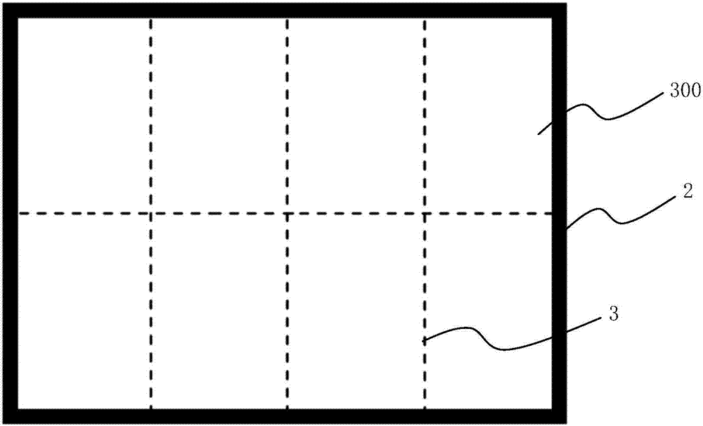
[0074] In this embodiment, the exposure of a large-scale FRD device is taken as an example to introduce the technical solution, and an FRD device with three types of regions is taken as an example for illustration. The large-size chip mentioned in this embodiment and the following embodiments refers to the chip 200 whose lithographic pattern size is larger than the exposure field size of the current mainstream lithography machine (generally 22mm*22mm). A specific embodiment of a power semiconductor chip exposure method, comprising the following steps:
[0075] S101) as attached Figure 6 As shown, according to the size of the exposure field of the lithography machine, the large-sized chip 200 is divided into several area units 300 by the dividing line 3, and the area unit 300 is divided into corner area units according to the type of the chip 200 (as shown in the attached Figure 6 Shown in A) 4, edge area unit (as attached Figure 6 shown in B) 5 and the central area unit (...
Embodiment 2
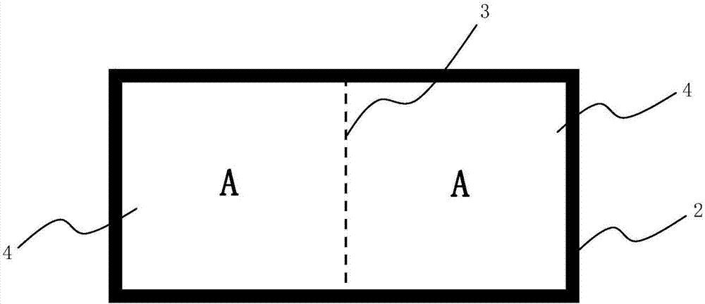
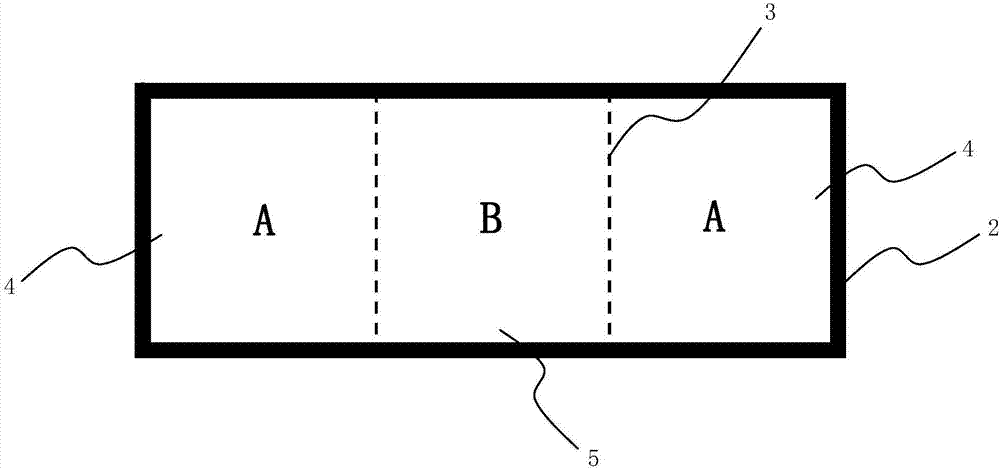
[0088] A specific embodiment of a power semiconductor chip photolithography plate, the photolithography plate 100 is composed of more than two square area units 300, and includes: an active area pattern 101, and a scribe line pattern located on the outer peripheral edge of the active area pattern 101 102 , the area unit 300 is divided by the large-sized chip 200 graphics through the dividing line 3 . The area unit 300 is divided into any type of corner area unit 4 , edge area unit 5 or central area unit 6 according to the type of graphics, and the internal graphics of the same type of area unit 300 are completely consistent. The reticle 100 includes all types of area units 300 divided by the chip 200 , and the size of the reticle 100 is smaller than or equal to that of the chip 200 . as attached Figure 6 To attach Figure 11 In the illustrated embodiment, the area unit 300 includes three types: the corner area unit 4, the edge area unit 5 and the center area unit 6, and the...
Embodiment 3
[0092] A specific embodiment of a power semiconductor chip, manufactured by the method described in Embodiment 1, the chip 200 is a large-sized FRD chip, and the structure of the chip 200 satisfies that the graphics at the junction of each area unit 300 are perpendicular to the boundary line 3, located at The patterns of the area units 300 on both sides of the boundary line 3 are consistent within a set range, which is larger than the positioning error of the light shield 7 of the photolithography machine. Specifically, it is suitable for large-scale FRD devices with the following vertical structure, mainly requiring that the boundary line 3 between the area units 300 is located in the middle of the pattern, and the distance between the two sides of the pattern is larger than the positioning error of the light shielding plate 7, so that Graphic shifting caused by positioning errors of the shading plate 7 can be avoided.
[0093] as attached Figure 14 Shown is a schematic dia...
PUM
 Abstract
Description
Claims
Application Information
 - R&D Engineer
- R&D Manager
- IP Professional
- Industry Leading Data Capabilities
- Powerful AI technology
- Patent DNA Extraction
Browse by: Latest US Patents, China's latest patents, Technical Efficacy Thesaurus, Application Domain, Technology Topic.
© 2024 PatSnap. All rights reserved.Legal|Privacy policy|Modern Slavery Act Transparency Statement|Sitemap