Eureka AIR delivers breakthrough ideas for toughest innovation challenges, trusted by R&D personnel around the world.

Method for detecting thinning of a semiconductor substrate of an integrated circuit from its backside and corresponding integrated circuit

A technology of integrated circuits and semiconductors, applied in the fields of semiconductor devices, semiconductor/solid-state device manufacturing, semiconductor/solid-state device components, etc., can solve the problem of increasing the efficiency of attacks, and achieve the effect of easy implementation

Active Publication Date: 2021-04-06
STMICROELECTRONICS (ROUSSET) SAS
View PDF7 Cites 0 Cited by
  • Summary
  • Abstract
  • Description
  • Claims
  • Application Information

AI Technical Summary

Problems solved by technology

[0004] The efficiency of this attack is increased when the substrate of the integrated circuit is thinned by the perpetrator from its backside in such a way as to be as close as possible to the components of the integrated circuit formed on its front side

Method used


Image

  • Method for detecting thinning of a semiconductor substrate of an integrated circuit from its backside and corresponding integrated circuit
  • Method for detecting thinning of a semiconductor substrate of an integrated circuit from its backside and corresponding integrated circuit

Examples


Embodiment Construction

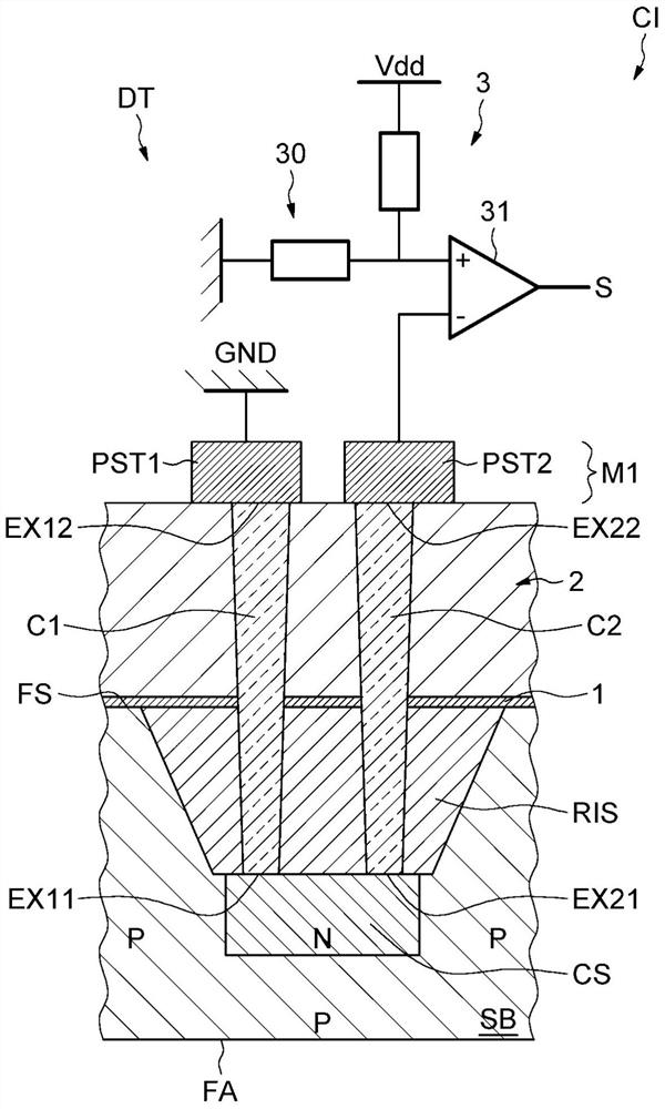
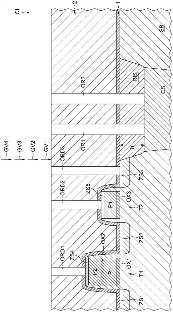
[0022] exist figure 1 , the reference IC designates an integrated circuit comprising, for example, a semiconductor substrate SB with P-type conductivity, including at least one insulating region RIS, for example of shallow trench isolation (STI) type, located in the example shown here with On top of the well CS of N conductivity type.

[0023] The top surface (or front side) FS of the substrate is covered by an etch stop layer 1 (CESL layer), typically silicon nitride SiN. This layer 1 is covered by a dielectric layer 2, usually designated by the person skilled in the art with the abbreviation PMD, which separates the etch stop layer 1 from the first metallization layer M1 of the interconnection part of the integrated circuit, the first metallization layer M1 of the interconnection part of the integrated circuit. A metallization layer M1 is usually designated by those skilled in the art with the abbreviation BEOL (for manufacturing back end of line).

[0024] In order to be ...


PUM


Abstract

Method for detecting thinning of a semiconductor substrate of an integrated circuit from its backside, comprising the measurement of terminals representing two conductive contacts (C1, C2) at the interface between an insulating region (RIS) and an underlying substrate region (CS) The physical quantity of electrical resistance between parts (EX11, EX21), said two conductive contacts (C1, C2) at least partly extend into said insulating region (RIS).

Description

technical field [0001] The present invention relates to integrated circuits, and more particularly to detecting potential thinning of integrated circuit substrates from their backsides. Background technique [0002] Integrated circuits, especially those equipped with memories containing sensitive information, must be protected as far as possible against attacks, in particular attacks designed to discover stored data. [0003] One possible attack can be achieved by a focused ion beam (FIB—Focused Ion Beam), for example by means of a laser beam. [0004] The effectiveness of this attack is increased when the substrate of the integrated circuit is thinned by the perpetrator from its backside in such a way as to be as close as possible to the components of the integrated circuit formed on its front side. Contents of the invention [0005] According to an embodiment and its implementation, a method is thus provided for detecting a possible thinning of a substrate of an integra...

Claims


Application Information

Patent Timeline
Patent Type & Authority Patents(China)
IPC IPC(8): H01L21/66H01L21/28
CPCH01L21/28H01L22/14H01L22/34G06F21/87H01L21/76898H01L21/823475H01L21/76829H10B69/00G11C16/22H01L21/31116H01L21/74H01L21/823481H01L21/823892H01L23/57H01L23/576H01L29/7846
Inventor P·弗纳拉C·里韦罗
Owner STMICROELECTRONICS (ROUSSET) SAS
Why Eureka
Eureka Blog
Learn More