Packaging structure, packaging method for OLED display device, and display device

A technology for display devices and packaging methods, applied in semiconductor devices, electric solid-state devices, organic light-emitting devices, etc., can solve the problems affecting the service life of OLED display devices, residual particles on the mask plate, etc., so as to reduce the mask plate alignment process, avoid Process assurance, the effect of saving packaging costs

Active Publication Date: 2017-08-29
BOE TECH GRP CO LTD +1
View PDF6 Cites 26 Cited by
  • Summary
  • Abstract
  • Description
  • Claims
  • Application Information

AI Technical Summary

Problems solved by technology

[0004] The object of the present invention is to provide a packaging structure, packaging method, and display device of an OLED display device, which are used to solve the problem that residual particles are easily generated on the edge of the mask board when the OLED display device is packaged, which affects the service life of the OLED display device. The problem

Method used


Image

  • Packaging structure, packaging method for OLED display device, and display device
  • Packaging structure, packaging method for OLED display device, and display device
  • Packaging structure, packaging method for OLED display device, and display device

Examples


Embodiment Construction

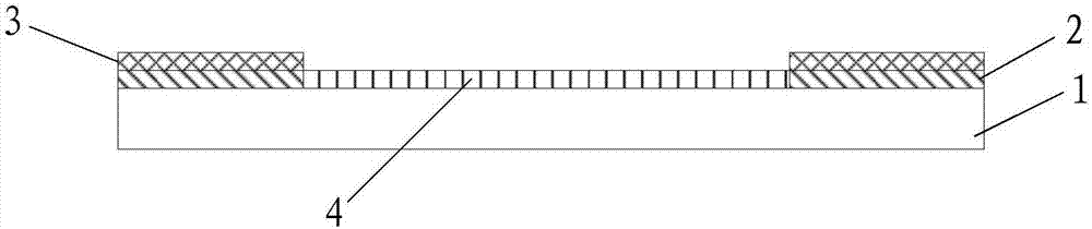
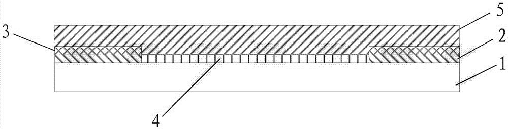
[0032] In order to further illustrate the encapsulation structure, encapsulation method, and display device of the OLED display device provided by the embodiments of the present invention, a detailed description will be given below in conjunction with the accompanying drawings.

[0033] As mentioned in the background technology, the traditional encapsulation process needs to use a mask board to cover the OLED display device to be encapsulated, and then use CVD technology or ALD technology to deposit an encapsulation film on the encapsulation area on the OLED display device to be encapsulated, so as to realize the OLED display device. package. CVD technology is a process technology that passes one or several compounds containing thin film elements and elemental gas into a reaction chamber where a substrate is placed, and deposits a solid film on the surface of a substrate by means of a space gas phase chemical reaction; The gas-phase precursor is alternately passed into the rea...


PUM


Abstract

The invention discloses a packaging structure, a packaging method for an OLED display device, and a display device, and relates to the field of display technologies, for solving the problem that when the OLED display device is packaged, residual particles are prone to generate at the edge of a mask plate, and thus service life of the OLED display device is influenced. The packaging method for the OLED display device comprises the steps of providing a substrate, wherein the substrate comprises a packaging area and a binding area positioned around the packaging area, and an electrode lead used for binding is arranged in the binding area; forming a sacrificial layer on the electrode lead; forming an OLED display device in the packaging area; forming packaging film covering all areas of the substrate; and removing the sacrificial layer to separate the sacrificial layer and the packaging film on the sacrificial layer from the substrate. The packaging method for the OLED display device provided the invention is used for packaging the OLED display device.

Description

technical field [0001] The invention relates to the field of display technology, in particular to a packaging structure of an OLED display device, a packaging method, and a display device. Background technique [0002] An OLED (Organic Light-Emitting Diode, Organic Light-Emitting Diode) display device has many advantages such as low energy consumption, high contrast ratio, wide viewing angle, etc., and is a display device that has attracted extensive attention at present. The OLED display device uses organic light-emitting materials to make the organic light-emitting layer. When electrons and holes recombine in the organic light-emitting layer, the organic light-emitting layer emits light, thereby realizing the display function of the OLED display device. Since organic light-emitting materials are sensitive to water and oxygen, after the OLED display device is manufactured, it needs to be packaged to isolate the organic light-emitting layer from external water and oxygen to ...

Claims


Application Information

Patent Timeline
Patent Type & Authority Applications(China)
IPC IPC(8): H01L51/52H01L51/56
CPCH10K50/8426H10K50/84H10K71/00H10K50/805H10K50/841H10K50/8445
Inventor 王玉林
Owner BOE TECH GRP CO LTD
Why Eureka
Try Eureka