OLED device and packaging method and packaging device thereof

A packaging method and a technology of a packaging device, which are applied in the manufacture of electric solid-state devices, semiconductor devices, semiconductor/solid-state devices, etc., can solve problems such as low productivity, adverse effects of devices, and impact on packaging effects, so as to improve quality and life, and improve packaging effect, quick and easy separation of effects

Active Publication Date: 2015-04-22
BOE TECH GRP CO LTD +1
View PDF8 Cites 12 Cited by
  • Summary
  • Abstract
  • Description
  • Claims
  • Application Information

AI Technical Summary

Problems solved by technology

[0004] UV glue encapsulation is a relatively common OLED device packaging method in the laboratory. It is low in cost and easy to operate. However, UV glue will contact the device during ultraviolet curing, causing adverse effects on the device, and cannot be applied in the actual industry.
Frit (glass glue) encapsulation method is a kind of encapsulation method that uses glass powder to solidify to connect the encapsulation glass to the substrate. It is a relatively mature encapsulation method in the industry. The disadvantage of this method is that the curing effect of the glass frit cannot be controlled. Cracks will appear during the curing process of glass powder, which will affect the packaging effect, and air will enter the device from the cracks, affecting the life of the device
In response to the defects of Frit packaging, the advantages of thin-film packaging have begun to emerge. Thin-film packaging is to package OLED devices by preparing organic and inorganic alternating multi-layer films on the cathode surface of OLED devices, but the packaging process of this method is too complicated, and Immature process and low productivity

Method used


Image

  • OLED device and packaging method and packaging device thereof
  • OLED device and packaging method and packaging device thereof
  • OLED device and packaging method and packaging device thereof

Examples


Embodiment 1

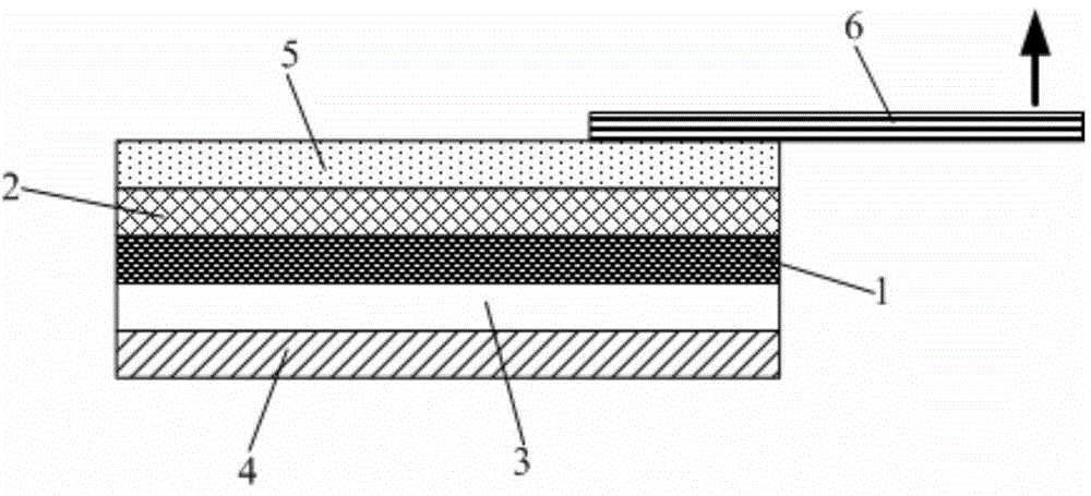
[0054] This embodiment provides a packaging method for packaging an OLED device formed on a substrate, including: separating the graphene film formed on the copper foil from the copper foil, and packaging the OLED device with the graphene film.

[0055] This encapsulation method can give full play to the characteristics of high light transmittance, ultra-thin and flexible, high water and oxygen barrier and easy transfer between substrates (that is, easy to separate from copper foil and connect with OLED devices) of graphene film. The introduction into the packaging of OLED devices not only improves the packaging effect of OLED devices, but also simplifies the packaging process of OLED devices and improves production efficiency.

[0056] In this embodiment, the graphene film formed on the copper foil is separated from the copper foil, and the OLED device is packaged by using the graphene film, which specifically includes: figure 1 and figure 2 as shown,

[0057] Step S10: Bo...

Embodiment 2

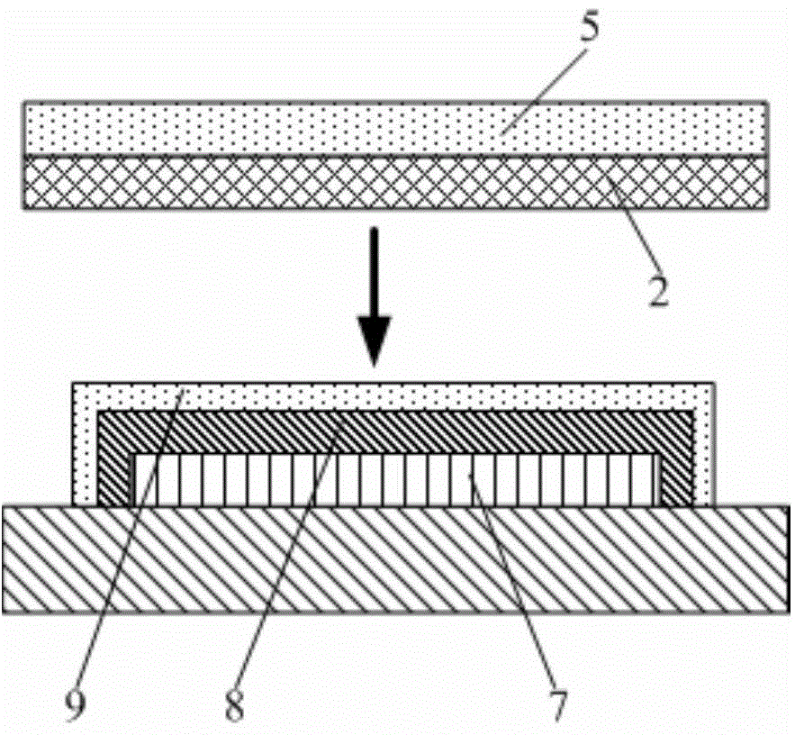
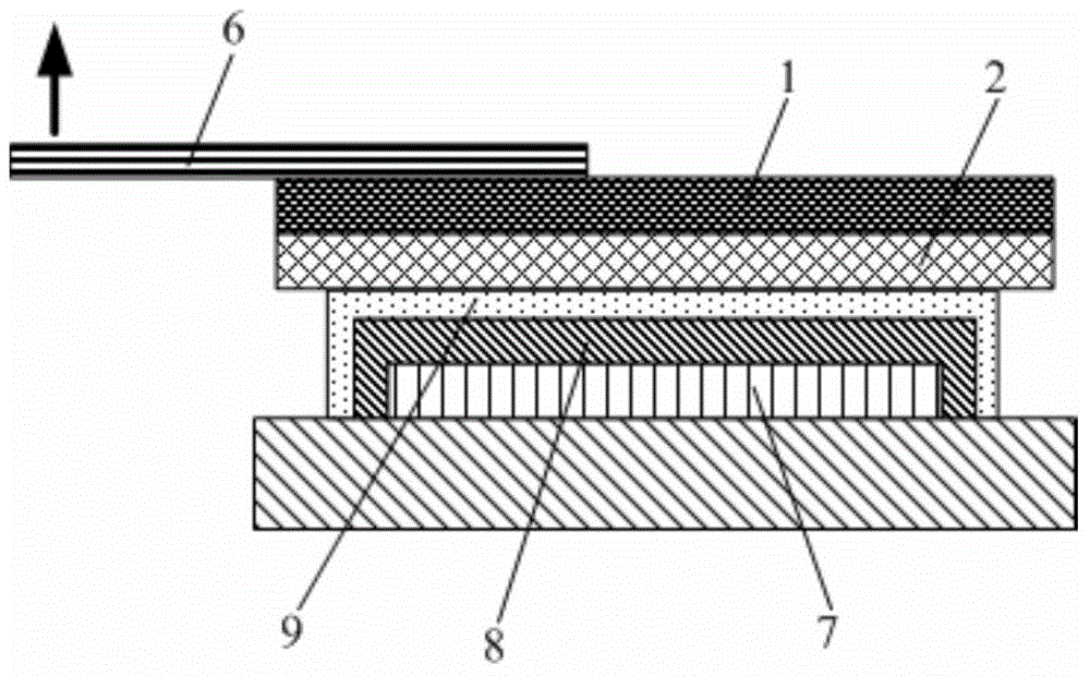
[0072] This embodiment provides a packaging method, which is different from Embodiment 1 in that the graphene film formed on the copper foil is separated from the copper foil, and the OLED device is packaged by using the graphene film, which specifically includes: image 3 and Figure 4 as shown,

[0073] Step S20 : ​​forming a passivation layer 8 on the OLED device 7 , and coating a transparent glue 9 on the passivation layer 8 .

[0074] The material of the transparent glue 9 is the same as in Example 1. The material and formation method of the passivation layer 8 are the same as those in Embodiment 1.

[0075] Step S21 : before the transparent glue 9 is cured, stick the side of the copper foil 1 on which the graphene film 2 is formed on the transparent glue 9 .

[0076] Step S22: curing the transparent glue 9 .

[0077] The curing temperature of the transparent glue 9 is the same as in Example 1.

[0078] Step S23: Fixing the OLED device 7 completed in step S22, sticki...

Embodiment 3

[0086] This embodiment provides a packaging method. The difference from Embodiment 1-2 is that the graphene film formed on the copper foil is separated from the copper foil, and the OLED device is packaged by using the graphene film. Specifically include: Figure 5 as shown,

[0087] Step S30 : forming a passivation layer 8 on the OLED device 7 .

[0088] The material and formation method of the passivation layer 8 are the same as those in Embodiment 1.

[0089] Step S31 : attaching the side of the copper foil 1 on which the graphene film 2 is not formed on the heated roller 11 .

[0090] A heating device is arranged inside the roller 11 , and the heating device can heat the axial surface of the roller 11 .

[0091] Step S32 : fixing the base substrate 12 completed in step S30 on the base 13 , with the OLED device 7 facing away from the base 13 .

[0092] In this step, the base substrate 12 completed in step S30 is fixed on the base 13 by the adhesive method or the vacuum a...


PUM


Abstract

The invention provides an OLED device and a packaging method and a packaging device thereof. The OLED device formed on a substrate base plate is packaged by using the packaging method. The packaging method comprises the following steps that grapheme film formed on copper foil is separated from the copper foil, and the grapheme film is used for packaging the OLED device. The packaging method can give full play to the grapheme film characteristic of being high in light transmittance, thin and flexible, high in water and oxygen isolation degree, and prone to being transferred among substrates which means the grapheme film is easy to be separated from the copper foil and connected with the OLED device; through introducing the grapheme film into the OLED device packaging, not only is the packaging effect of the OLED device improved, but also the packaging technology of the OLED device is simplified, and the production efficiency is improved.

Description

technical field [0001] The present invention relates to the field of display technology, in particular to an OLED device, a packaging method and a packaging device thereof. Background technique [0002] With the continuous maturity of organic electroluminescence (OLED) technology, the continuous evolution of OLED equipment, and the packaging method and packaging level of OLED devices have always been key topics in the industry. [0003] Because water and oxygen are the natural enemies of organic materials, they can not only open the unsaturated bonds of polymers, accelerate the aging of organic materials, but also cause damage to the electrodes in the device. The packaging level of OLED devices determines the lifetime and environmental reliability of the devices. [0004] UV glue encapsulation is a relatively common OLED device packaging method in the laboratory. It is low in cost and easy to operate. However, UV glue will contact the device during ultraviolet curing, causi...

Claims


Application Information

Patent Timeline
Patent Type & Authority Applications(China)
IPC IPC(8): H01L51/52H01L51/56
CPCH10K50/84H10K71/00B32B9/04B32B9/045B32B27/06B32B27/28B32B27/283B32B27/302B32B27/304B32B27/32B32B27/36B32B27/365B32B27/38B32B27/40B32B27/42B32B2255/00B32B2255/20B32B2255/24B32B2255/26B32B2255/28B32B2270/00B32B2307/546B32B2307/7244B32B2307/7265B32B2307/748B32B2553/00B32B7/12B32B2457/206H10K50/844H10K2102/00B32B9/041
Inventor 冯翔王涛邱云
Owner BOE TECH GRP CO LTD
Why Eureka
Try Eureka