

Organic electroluminescent device and method for producing same
An electroluminescence device and electroluminescence technology, which are applied in the manufacturing of organic semiconductor devices, electric solid state devices, and semiconductor/solid state devices, etc., can solve the problems of device temperature rise, insufficient packaging, poor heat dissipation, etc., and achieve tight and good sealing. Packaging effect, good heat dissipation effect
- Summary
- Abstract
- Description
- Claims
- Application Information
AI Technical Summary
Problems solved by technology
Method used
Image

Examples
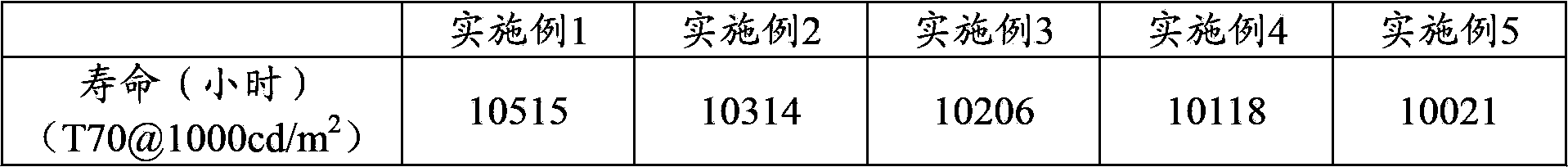
Embodiment 1
[0055] A method for preparing an organic electroluminescent device, including the following steps:
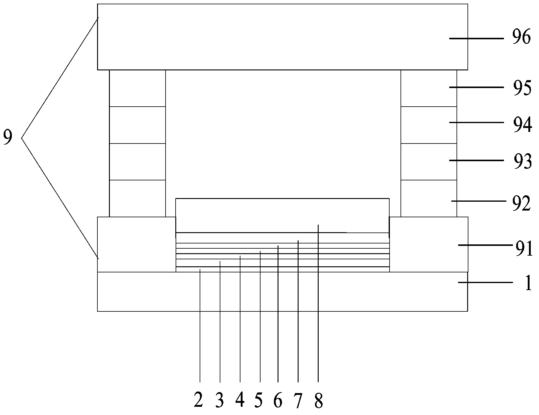
[0056] (1) Pretreatment of the anode conductive substrate 1: the anode conductive substrate 1 is an indium tin oxide (ITO) glass substrate, acetone cleaning→ethanol cleaning→deionized water cleaning→ethanol cleaning, all are cleaned with an ultrasonic cleaning machine, a single cleaning 5 minutes, then blow dry with nitrogen, and oven dry for later use; the cleaned anode conductive substrate 1 needs to be surface activated to increase the oxygen content of the conductive surface layer and improve the work function of the conductive layer surface; The thickness of the conductive substrate 1 is 100 nm;
[0057] (2) Preparation of functional layer and light-emitting layer:
[0058] Hole injection layer 2: The hole injection layer 2 is vacuum-evaporated on the surface of the anode conductive substrate 1 by covering the mask. The mask is arranged around the edge of the upper surface of th...
Embodiment 2
[0072] A method for preparing an organic electroluminescent device, including the following steps:
[0073] (1), (2), (3) are the same as in Example 1;
[0074] (4) Preparation of protective layer: A protective layer with the same size as the cathode layer is prepared on the surface of the cathode layer by vacuum evaporation. The material of the protective layer is NPB, and the vacuum degree is 5×10. -5 Pa, evaporation rate Thickness 300nm;
[0075] (5) Preparation of the insulating layer: The insulation surrounding the hole injection layer, hole transport layer, light emitting layer, electron transport layer, electron injection layer, cathode layer and protective layer is set on the anode conductive substrate by magnetron sputtering. Layer, insulating layer material is Al 2 O 3 , The target is Al 2 O 3 , The background vacuum is 5×10 -5 Pa, enter Ar, flow rate is 5sccm, the radial width of the insulating layer is 3mm, and the thickness is 200nm;
[0076] (6) Preparation of the first...
Embodiment 3
[0081] A method for preparing an organic electroluminescent device, including the following steps:
[0082] (1), (2), (3) are the same as in Example 1;
[0083] (4) Preparation of protective layer: A protective layer with the same size as the cathode layer is prepared on the surface of the cathode layer by vacuum evaporation, and the material of the protective layer is Alq 3 , The vacuum degree is 5×10 -5 Pa, the evaporation rate is The thickness is 250nm;
[0084] (5) Preparation of the insulating layer: The insulation surrounding the hole injection layer, hole transport layer, light emitting layer, electron transport layer, electron injection layer, cathode layer and protective layer is set on the anode conductive substrate by magnetron sputtering. Layer, the insulating layer is made of Si 3 N 4 , The target is Si 3 N 4 , The background vacuum is 5×10 -5 Pa, enter Ar, the flow rate is 5sccm, the radial width of the insulating layer is 4mm, and the thickness is 200nm;
[0085] (6) P...
PUM
| Property | Measurement | Unit |
|---|---|---|
| thickness | aaaaa | aaaaa |
| width | aaaaa | aaaaa |
| thickness | aaaaa | aaaaa |
Abstract
Description
Claims
Application Information