elastic wave device
A technology of elastic wave devices and capacitive elements, applied in the direction of impedance network, electrical components, etc., which can solve the problems of elastic wave device characteristics degradation and increased manufacturing cost
- Summary
- Abstract
- Description
- Claims
- Application Information
AI Technical Summary
Problems solved by technology
Method used
Image

Examples
no. 1 Embodiment approach
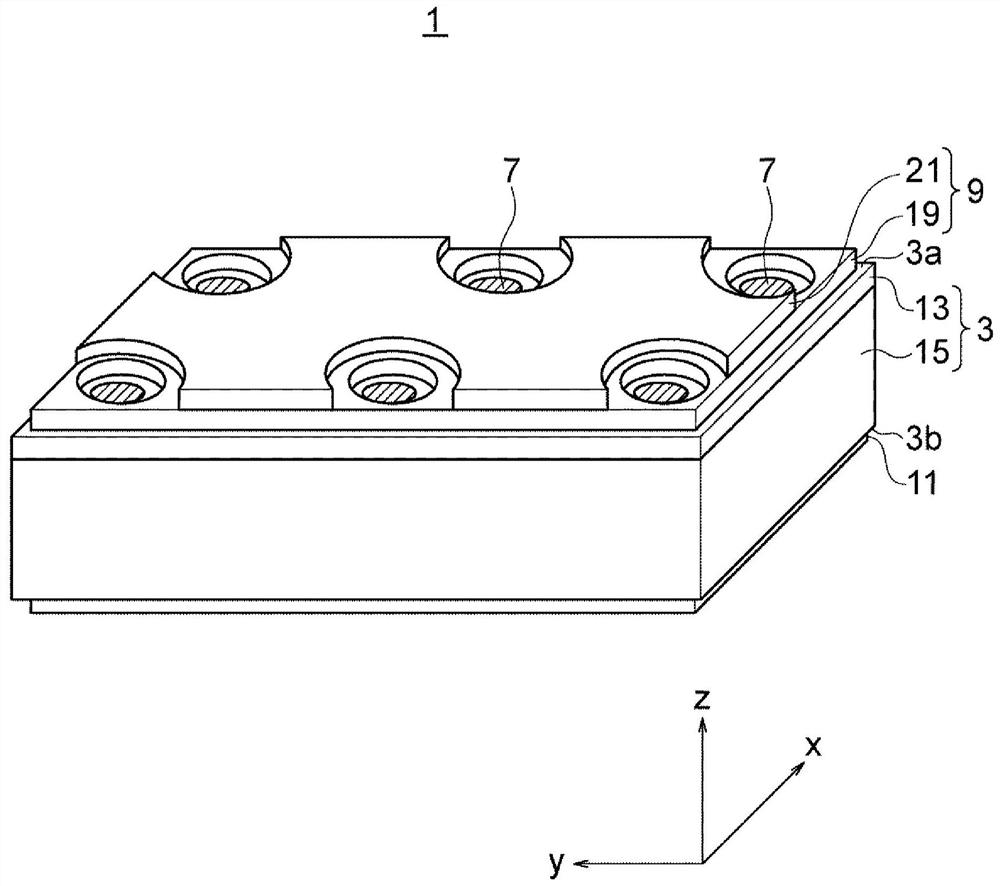
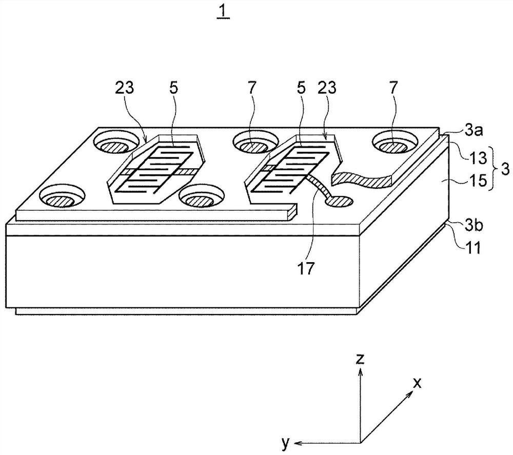
[0030] figure 1 It is an external perspective view of the SAW device 1 according to the first embodiment of the present invention. also, figure 2 It is a perspective view showing a part of the SAW device 1 cut away.
[0031] The SAW device 1 may use any direction as up or down, but in the following embodiments, sometimes for convenience, an orthogonal coordinate system xyz is defined, and the positive side of the z direction ( figure 1 The upper side of the paper surface) as the upper side, terms such as upper surface and lower surface are used. In addition, the orthogonal coordinate system xyz is defined based on the shape of the SAW device 1 , and does not refer to the electrical axis, mechanical axis, and optical axis of the piezoelectric substrate.
[0032] The SAW device 1 is, for example, a relatively small substantially rectangular parallelepiped electronic component. Its size can be appropriately set, for example, the thickness is 0.1 mm to 0.4 mm, and the length ...
no. 2 Embodiment approach
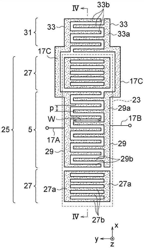
[0098] Figure 5 (a) is a plan view showing the SAW resonator 25 and the capacitive element 31 of the SAW device according to the second embodiment.
[0099] The second embodiment differs from the first embodiment only in the orientation of the capacitive element 31 . That is, in the second embodiment, the capacitive element 31 is arranged such that the angle θ of the electrode fingers 33b with respect to the electrode fingers 29b of the IDT electrode 5 is larger than 0° and smaller than 90°. In other words, the electrode fingers 33b are inclined relative to the electrode fingers 29b. Furthermore, the bus bar 33a of the capacitive element 31 is also inclined with respect to the bus bar 29a of the IDT electrode 5 at the same angle as the angle between the electrode finger 33b and the electrode finger 29b.
[0100] As described above, the smaller the angle θ is, the more the insertion loss caused by the capacitive element 31 can be reduced, but on the other hand, the spur beco...
no. 3 Embodiment approach
[0103] Figure 5 (b) is a plan view showing the SAW resonator 25 and the capacitive element 331 of the SAW device according to the third embodiment.
[0104] The third embodiment differs from the first embodiment in that electrode fingers 333 b of capacitive elements 331 (capacitive electrodes 333 ) are inclined with respect to electrode fingers 29 b of IDT electrodes 5 as in the second embodiment. However, in the third embodiment, unlike the second embodiment, the bus bar 333a of the capacitive element 331 is parallel to the bus bar 29a of the IDT electrode 5 . From another point of view, the second embodiment differs from the first embodiment in that the electrode fingers 333b of the capacitive element 331 extend obliquely with respect to the opposing direction (y direction) of the bus bar 333a of the capacitive element 331 .
[0105] In this configuration, firstly, since the electrode fingers 333b of the capacitive element 331 are inclined with respect to the electrode fin...
PUM
 Abstract
Description
Claims
Application Information
 - R&D Engineer
- R&D Manager
- IP Professional
- Industry Leading Data Capabilities
- Powerful AI technology
- Patent DNA Extraction
Browse by: Latest US Patents, China's latest patents, Technical Efficacy Thesaurus, Application Domain, Technology Topic.
© 2024 PatSnap. All rights reserved.Legal|Privacy policy|Modern Slavery Act Transparency Statement|Sitemap