High performance optoelectronic packaging assembly

a packaging assembly, optoelectronic technology, applied in the direction of optical elements, semiconductor lasers, instruments, etc., can solve the problems of signal flow issues that still require the full attention and creativity of designers, device size has not solved fundamental signal flow bottlenecks, and the overall system bandwidth remains limited. , to achieve the effect of simple, accurate and stable optical alignment, good thermal performance and convenient mounting of optoelectronic devices

Inactive Publication Date: 2006-07-04
SILICON BANDWIDTH
View PDF10 Cites 19 Cited by
  • Summary
  • Abstract
  • Description
  • Claims
  • Application Information

AI Technical Summary

Benefits of technology

[0014]An advantage of the present invention is to provide for optoelectronic packaging assemblies that support easy mounting of optoelectronic devices, relatively simple, accurate and stable optical alignment between a packaged optoelectronic device and an optical fiber, good thermal performance, and improved high-speed electrical characteristics. In particular, the principles of the present invention provide for optoelectronic packaging assemblies having improved adjacent pin isolation, improved radiation suppression, reduced noise, reduced signal reflections, and reduced resonance.
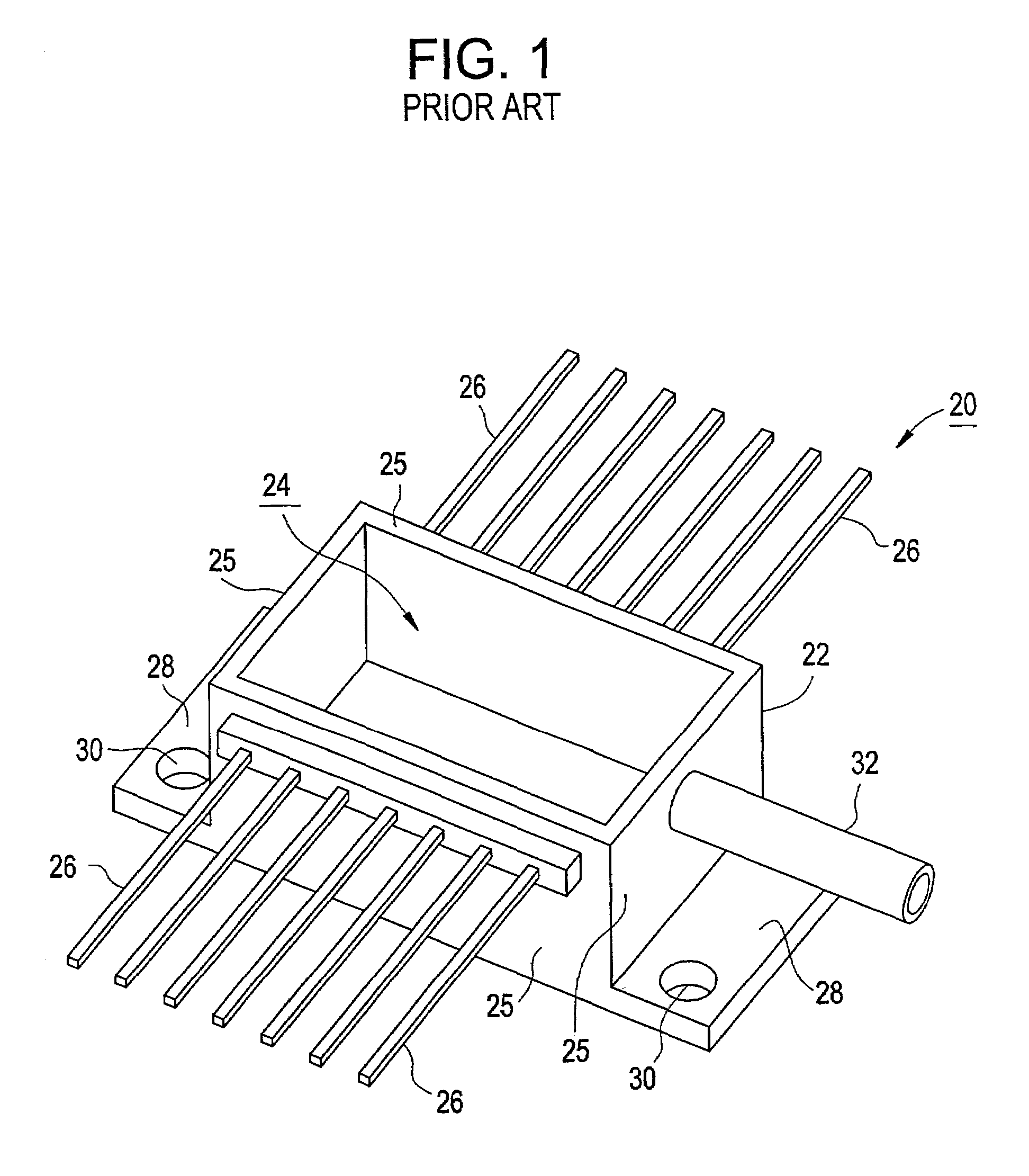
[0015]Beneficially, such optoelectronic packaging assemblies are implemented as enhanced replacements for traditional butterfly packages. Instead of KOVAR (used in many prior art packages), optoelectronic packaging assemblies in accord with the present invention are beneficially fabricated from nonconductive plastic, such as liquid crystal polymers (LCP). Instead of simple electrical leads, connections to optoelectronic packaging assemblies in accord with the present invention are made using transmission line pins comprised of an inner conductor, a dielectric sheath, and a conductive outer shield. Electromagnetic shielding, chassis ground, and tight control of radiated emissions are implemented by employing surface metallization on the nonconductive plastics (LCP). To further enhance electrical performance, optoelectronic packaging assemblies in accord with the present invention avoid large interior cavities that can have resonance frequencies on the same order as the operating speeds (i.e. 5–40 GHz). Furthermore, optoelectronic packaging assemblies in accord with the present invention beneficially include molded breaks, steps, and angled walls that reduce the parallel plate wave guide modes excited between the package walls.
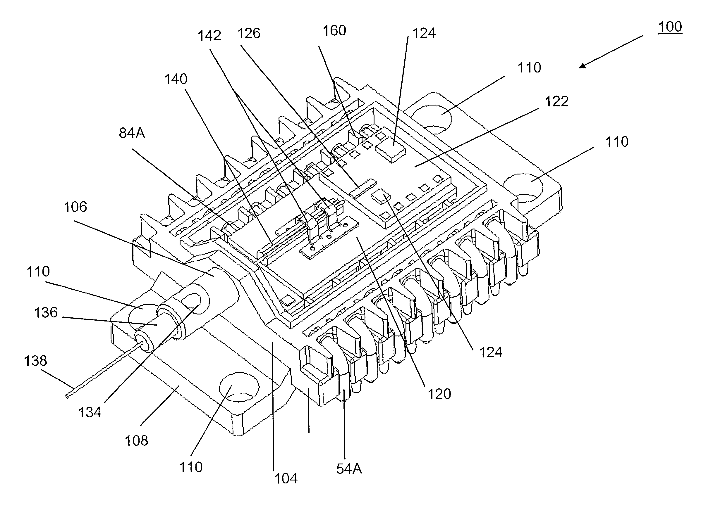
[0016]A first embodiment optoelectronic packaging assembly that is in accord with the principles of the present invention includes a cover, a submount, and a base that are beneficially comprised of nonconductive plastic having a conductive coating or plating over a surface. The submount retains a plurality of transmission line pins that extend from a cavity within the submount to the exterior. The transmission line pins are each comprised of an inner conductor encased by a dielectric sheath that is surrounded by a conductive outer shield. The first embodiment optoelectronic packaging assembly further includes an optical input receptacle for retaining an optical fiber. The cover, submount and base fit together to form a package. Beneficially, the nonconductive plastic is a liquid crystal polymer. Furthermore, beneficially, the cover includes beveled walls and / or heat sink fins. A thermal electric cooler is optional.
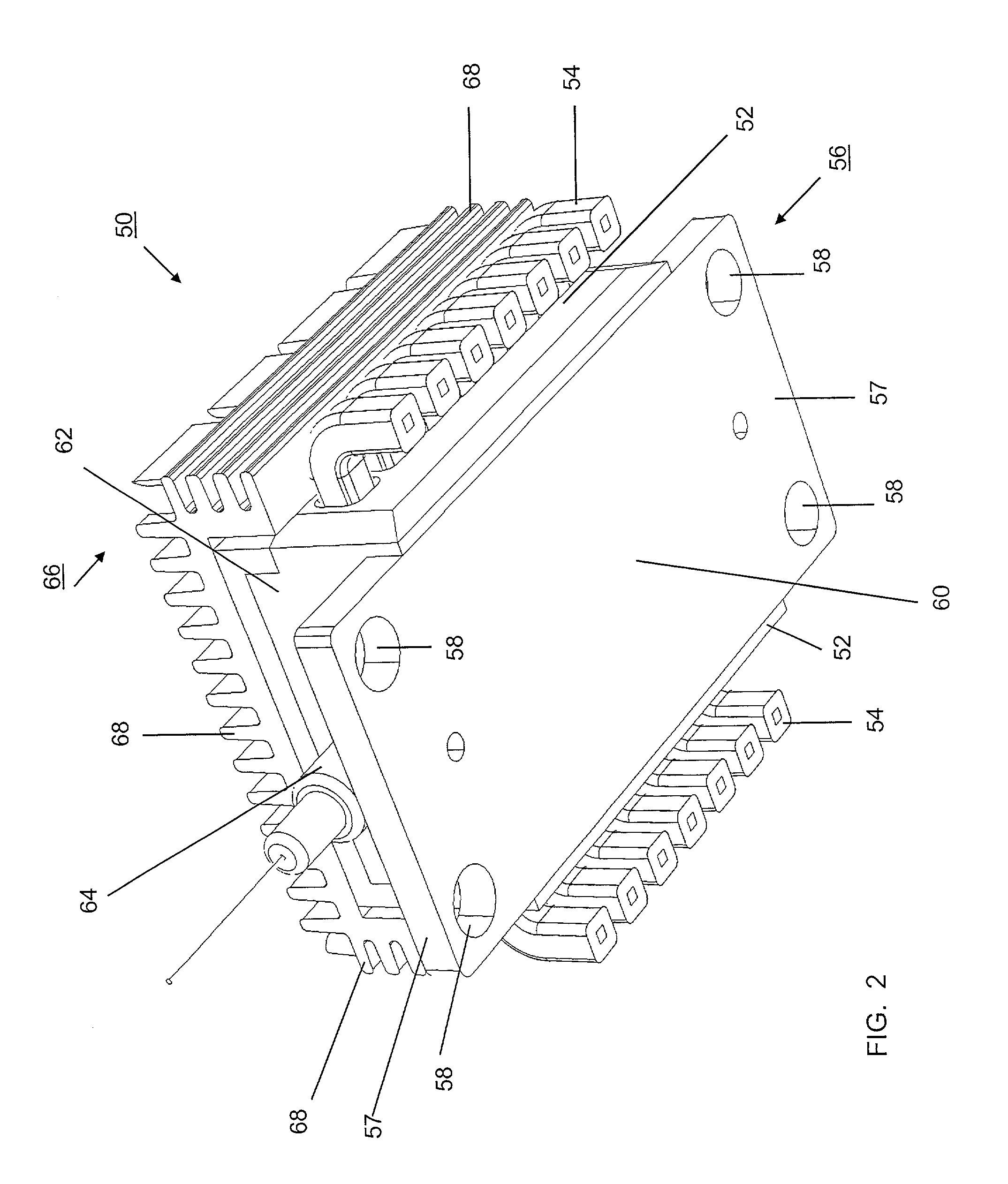
[0017]A second embodiment optoelectronic packaging assembly that is in accord with the principles of the present invention includes a cover, a submount, and a base that are beneficially comprised of nonconductive plastic having a conductive coating or plating over a surface. The submount retains a plurality of transmission line pins that extend from a cavity. The transmission line pins are each comprised of an inner conductor encased by a dielectric sheath that is surrounded by a conductive outer shield. The submount further includes barriers between adjacent transmission line pins. Those barriers have a conductive material over a surface. The cover, submount, and base form a package that beneficially electrically shields the cavity, which preferably includes beveled walls and / or heat sink fins. Beneficially, the nonconductive plastic is beneficially a liquid crystal polymer. The base can include a thermally conductive plate, beneficially a plate that mates with an external structure. A thermal electric cooler is optional.
[0018]A third embodiment optoelectronic packaging assembly that is in accord with the principles of the present invention includes a cover, a submount, and a base that are beneficially comprised of nonconductive plastic having a conductive coating or plating over a surface. The submount retains a plurality of transmission line pins that extend from a cavity within the submount to the exterior. The transmission line pins are each comprised of an inner conductor encased by a dielectric sheath that is surrounded by a conductive outer shield. The first embodiment optoelectronic packaging assembly further includes an optoelectronic device disposed between the submount and the base. Also included is an optical input receptacle for retaining an optical fiber. The cover, submount and base fit together to form a package. Beneficially, the nonconductive plastic is a liquid crystal polymer. The transmission line pins preferably bend in the direction of the base. Beneficially, the cover includes beveled walls and / or heat sink fins. A thermal electric cooler is optional.
[0019]The novel features of the present invention will become apparent to those of skill in the art upon examination of the following

Problems solved by technology

Despite advances in data- and telecommunications systems, overall system bandwidths remain limited by the need to interconnect various system modules.
Decreasing device sizes have not solved fundamental signal flow bottlenecks, the problems have only shifted to package, module, and interconnection levels.
Despite rapid improvements in electromagnetic simulation tools and increasing computational power, signal flow issues still requires a designer's full attention and creativity in the research and development phases.
One significant problem is coupling with the required alignment accuracy and stability over time and temperature.
Manually aligning optical components with optical fibers is time consuming and costly.
Because of the extremely high frequencies of the light used in optical systems, such systems can potentially operate with exceptionally wide bandwidths.
Unfortunately, the electrical systems required to actually use the available bandwidth are often difficult to implement.
For example, most prior art optoelectronic packages when operated at GHz frequencies have excessive dielectric signal losses.
Furthermore, electrical signal reflections caused by impedance mismatches at the package can be seriously detrimental to system performance.
Additionally, undesired electrical resonance can exist inside an optoelectronic package, resulting in a poor performance.
Unfortunately, such materials often have undesirable cost, thermal, and molding characteristics.
For example, polytetrafluoroethylene, which has very low dielectric loss, may be too expensive for some application and can be difficult to mold.
To reduce line reflections, the optoelectronic package should have carefully controlled input impedances, but this has been very difficult to do, particularly in mass-produced optoelectronic packaging assemblies.
While the package 20 is generally successful, it suffers from various limitations.
First, such optoelectronic packaging assemblies generally have poor heat dissipation characteristics.
Second, the walls 25 tend to be relatively high, thus increasing the difficulty of mounting and then electrically and optically interconnecting a contained optoelectronic component or assembly with an optical fiber.
Other limitations of the package 20 are its relatively poor control of the impedance of the pins 26, a susceptibility to internal resonance, and signal radiation and / or noise pick-up.

Method used


Image

  • High performance optoelectronic packaging assembly
  • High performance optoelectronic packaging assembly
  • High performance optoelectronic packaging assembly

Examples


Embodiment Construction

[0039]References will now be made in detail to various embodiments of the present invention, examples of which are illustrated in the accompanying drawings. Those embodiments relate to novel, unobvious, and useful optoelectronic packaging assemblies. Typically, all body components (such as covers, base, and submount) of the illustrated optoelectronic packaging assemblies are molded from a liquid crystal polymer (such as VECTRA). Those body components are beneficially plated or coated with a conductive material, preferably on both internally and externally. The conductive material electrically connects various features (such as subsequently described transmission line pin shields and cover cavity walls) to electrical ground. The conductive material further provides for electrical shielding that isolates devices within the optoelectronic packaging assemblies from exterior elements, while also reducing or eliminating electrical resonance within the optoelectronic packaging assemblies. ...


PUM


Abstract

Optoelectronic packaging assemblies for optically and electrically interfacing a protected electro-optical device or system to both an optical fiber and to external circuitry. Such assemblies are comprised of body components that are comprised of plastic that coated or plated with a conductive material. Electrical contact pins in the form of transmission lines are used to couple external electrical signals with the package. The optoelectronic packaging assemblies are dimensioned with small cavities and with steps, breaks, walls, and / or fins molded into the body components. The optoelectronic packaging assemblies further include an optical input receptacle for receiving an optical ferrule and an optical fiber. The optoelectronic packaging assembly provides for cooling, such as by heat sink fins and / or a thermal-electric-cooler. The transmission line pins and body components are dimensioned to mate with a standardized circuit board having transmission line traces.

Description

CROSS-REFERENCE TO RELATED APPLICATIONS[0001]This is a continuation-in-part of U.S. patent application Ser. No. 09 / 940,649, which was filed on Aug. 29, 2001, and is now U.S. Pat. No. 6,663,294.BACKGROUND OF THE INVENTION[0002]1. Field of the Invention[0003]This invention relates to the packaging of optoelectronic devices. More particularly, the present invention relates to optoelectronic packaging assemblies that provide for optical coupling, cooling, and high-speed electrical operations.[0004]2. Discussion of the Related Art[0005]Despite advances in data- and telecommunications systems, overall system bandwidths remain limited by the need to interconnect various system modules. Decreasing device sizes have not solved fundamental signal flow bottlenecks, the problems have only shifted to package, module, and interconnection levels. Despite rapid improvements in electromagnetic simulation tools and increasing computational power, signal flow issues still requires a designer's full at...

Claims


Application Information

Patent Timeline
Patent Type & Authority Patents(United States)
IPC IPC(8): G02B6/42G02B6/38H01S5/022H01S5/024
CPCG02B6/3839G02B6/4201G02B6/4228G02B6/4277H01S5/02216H01S5/02415G02B6/4248G02B6/423H01S5/02469H01S5/02284G02B6/4251G02B6/4255G02B6/4265G02B6/4271G02B6/424G02B6/4269G02B6/4274H01S5/02251
Inventor CRANE, JR., STANFORD W.JEON, MYOUNG-SOONICKEL, JOSHUA G.HORVATH, ZSOLT
Owner SILICON BANDWIDTH
Why Eureka
Try Eureka