
LED wafer cleaning device

A technology for cleaning wafers and cleaning boxes, which is applied to heating devices, cleaning methods and tools, cleaning methods using tools, etc. It can solve the problems of poor cleaning effect, affecting the performance of LED chips, troublesome use, etc., and achieves convenient and effective cleaning. excellent effect

Inactive Publication Date: 2017-09-15
FOSHAN ZHENGLUE INFORMATION TECH CO LTD
View PDF8 Cites 15 Cited by
  • Summary
  • Abstract
  • Description
  • Claims
  • Application Information

AI Technical Summary

Problems solved by technology

[0003] LED chip is a semiconductor device, and LED chip is the raw material for producing LED chip. In the later stage of chip production, the chip needs to be cleaned after being ground. The existing chip cleaning device is not only troublesome to use, but also has poor cleaning effect and affects Performance of LED chips

Method used


Image

  • LED wafer cleaning device
  • LED wafer cleaning device

Examples


Embodiment Construction

[0016] The following will clearly and completely describe the technical solutions in the embodiments of the present invention with reference to the accompanying drawings in the embodiments of the present invention. Obviously, the described embodiments are only some, not all, embodiments of the present invention. Based on the embodiments of the present invention, all other embodiments obtained by persons of ordinary skill in the art without making creative efforts belong to the protection scope of the present invention.

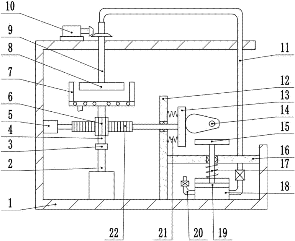
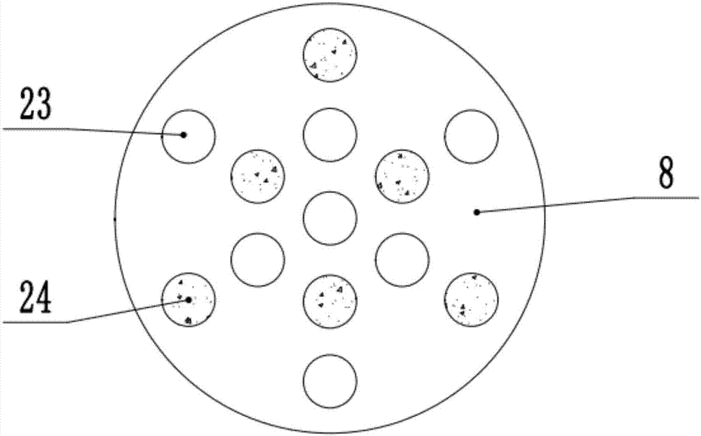
[0017] see Figure 1~2 , in an embodiment of the present invention, a LED wafer cleaning device includes a frame 1, a cleaning box 7, a cleaning disc 8, a first T-shaped bar 13 and a second T-shaped bar 15; the bottom of the frame 1 is fixed A hydraulic telescopic rod 2 is installed, and the cleaning box 7 is a box structure with an upper end opening. The bottom of the cleaning box 7 is fixedly equipped with a connecting rod 4, and the other end of the connect...


PUM


Abstract

The invention discloses an LED wafer cleaning device. The LED wafer cleaning device comprises a frame, a cleaning box, a cleaning disc, a first T-type rod and a second T-type rod; a connecting rod is fixedly mounted on the bottom of the cleaning box, and the other end of the connecting rod is rotatably connected with a telescopic end of a hydraulic telescopic rod through a ball bearing; a gear which drives the connecting rod to rotate is fixedly mounted on the connecting rod, and a rack is arranged on the rear side of the gear; the other end of the first T-type rod penetrates through a vertical baffle plate to the left and is fixedly connected with the right end of the rack; a cam is further rotatably arranged on the right side of the first T-type rod; a rotating shaft is rotatably arranged on the upper side of the frame, and the cleaning disc is fixedly connected to the lower side of the rotating shaft; and a water tank is further fixedly arranged on the bottom of the frame. According to the LED wafer cleaning device, through arranging the rotatable cleaning box and cleaning disc, cleaning is convenient and cleaning effect is excellent; and a heating plate is further arranged at the bottom of the cleaning box, so that the cleaned wafer can be dried.

Description

technical field [0001] The invention relates to the technical field of LED manufacturing equipment, in particular to an LED wafer cleaning device. Background technique [0002] At present, the domestic LED industry is showing a trend of rapid development, and the market is gradually becoming mature, mainly manifested in the fact that the price of LED products is getting lower and lower, and the performance is getting better and better. Most chip manufacturers have taken measures to expand scale, reduce costs, and improve quality to improve market competitiveness. [0003] LED chip is a semiconductor device, and LED chip is the raw material for producing LED chip. In the later stage of chip production, the chip needs to be cleaned after being ground. The existing chip cleaning device is not only troublesome to use, but also has poor cleaning effect and affects Performance of LED chips. Contents of the invention [0004] The object of the present invention is to provide an...

Claims


Application Information

Patent Timeline
IPC IPC(8): B08B3/02B08B1/02F26B23/00
CPCF26B23/00B08B3/022B08B1/20B08B1/12
Inventor 钟云华
Owner FOSHAN ZHENGLUE INFORMATION TECH CO LTD
Features
  • Generate Ideas
  • Intellectual Property
  • Life Sciences
  • Materials
  • Tech Scout
  • Unparalleled Data Quality
  • Higher Quality Content
  • 60% Fewer Hallucinations
Learn More