Manufacturing method of array substrate and manufacturing method of display device

A manufacturing method and array substrate technology, which are applied in the fields of final product manufacturing, sustainable manufacturing/processing, semiconductor/solid-state device manufacturing, etc., can solve problems such as increased production costs, threshold voltage drift, and long production cycles of flexible OLEDs. Effects of production cycle, reduction of production cost, and avoidance of threshold voltage drift

Active Publication Date: 2019-07-16
BOE TECH GRP CO LTD
View PDF5 Cites 0 Cited by
  • Summary
  • Abstract
  • Description
  • Claims
  • Application Information

AI Technical Summary

Problems solved by technology

[0004] The production cycle of the above-mentioned flexible OLED manufacturing method is relatively long, resulting in an increase in production cost
Moreover, when making the isolation layer and the isolation column, due to the need for two photolithography processes, the energy of the second exposure is too large, resulting in a threshold voltage shift (Vth shift) of the TFT due to a large area of ​​ultraviolet radiation.

Method used


Image

  • Manufacturing method of array substrate and manufacturing method of display device
  • Manufacturing method of array substrate and manufacturing method of display device
  • Manufacturing method of array substrate and manufacturing method of display device

Examples


Embodiment Construction

[0038] In order for those skilled in the art to better understand the technical solution of the present invention, the method for manufacturing the array substrate and the method for manufacturing the display device provided by the present invention will be described in detail below with reference to the accompanying drawings.

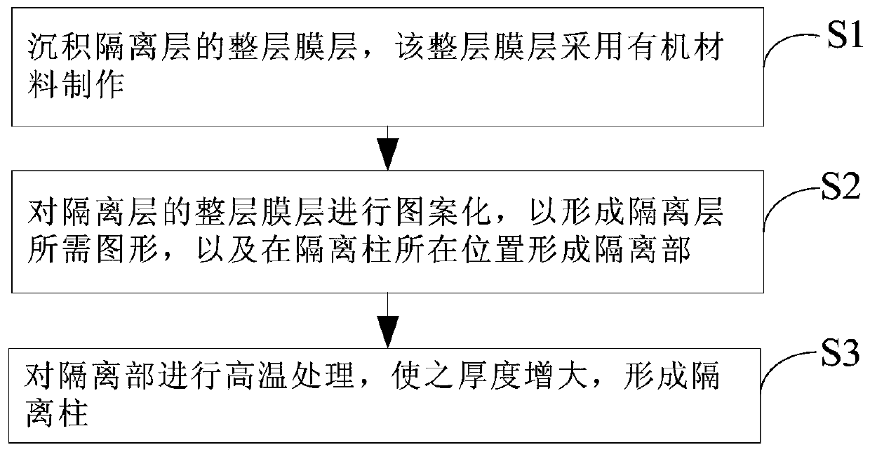
[0039] figure 1 It is a block flow diagram of the manufacturing method of the array substrate provided by the first embodiment of the present invention. see figure 1 , the manufacturing method of the array substrate includes:

[0040] Making the isolation column while making the isolation layer specifically includes the following steps:

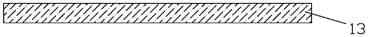
[0041] S1, forming the film 13 of the isolation layer, the film 13 of the isolation layer is made of organic materials, such as Figure 2A shown.

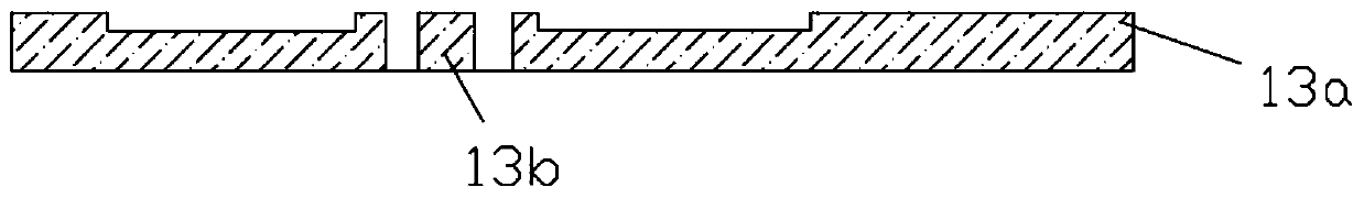
[0042] S2, patterning the thin film 13 of the isolation layer to form the required pattern 13a and isolation portion 13b of the isolation layer, such as Figure 2B sh...


PUM


Abstract

The present invention provides a manufacturing method of an array substrate and a display device, which include: manufacturing an isolation column while manufacturing an isolation layer; specifically including the following steps: S1, forming a thin film of the isolation layer, the thin film of the isolation layer is made of organic Material production; S2, patterning the thin film of the isolation layer to form the pattern required for the isolation layer and the isolation part; S3, performing high-temperature treatment on the isolation part to increase its thickness to form an isolation column. The manufacturing method of the array substrate provided by the present invention can not only shorten the production cycle and reduce the production cost, but also can avoid the threshold voltage drift of TFTs caused by the irradiation of large-area ultraviolet rays.

Description

technical field [0001] The present invention relates to the field of display technology, in particular, to a method for manufacturing an array substrate and a method for manufacturing a display device. Background technique [0002] Organic light-emitting diode (OLED) display technology is widely used in mobile phones, digital video cameras, DVD players, personal digital assistants (PDAs), notebook computers, car audio and televisions, and so on. At present, OLED products are mainly realized through 9 mask steps. [0003] The structure of the existing flexible OLED mainly includes a substrate and a guiding film layer, a transition layer, an active layer, two gates, a connecting layer, a source and a drain, a planar layer, an electrode layer, an isolation layer, and layers and spacers. Among them, the manufacturing method of the above-mentioned flexible OLED is mainly through the photolithography process of 9 masks, which are the active layer, two gates, the connection layer...

Claims


Application Information

Patent Timeline
Patent Type & Authority Patents(China)
IPC IPC(8): H01L51/56H01L27/32
CPCH10K59/12H10K2102/311H10K71/00Y02E10/549Y02P70/50H10K59/123H10K59/1213H10K77/111H10K50/8428H10K59/1201H10K59/87H10K50/84
Inventor 刘文渠董立文张锋吕志军党宁张世政
Owner BOE TECH GRP CO LTD
Why Eureka
Try Eureka