Flexible display substrate, manufacturing method thereof, and flexible display device

A flexible display and flexible substrate technology, applied in semiconductor/solid-state device manufacturing, electrical components, electrical solid-state devices, etc., can solve problems such as abnormal display, thin-film transistor threshold voltage drift, thin-film transistor characteristic failure, etc., to avoid display effect The effect of reducing, avoiding threshold voltage drift, and avoiding damage

Active Publication Date: 2016-11-30
BOE TECH GRP CO LTD
View PDF7 Cites 0 Cited by
  • Summary
  • Abstract
  • Description
  • Claims
  • Application Information

AI Technical Summary

Problems solved by technology

[0005] The present invention provides a flexible display substrate, its manufacturing method and a flexible display device, which are used to avoid the threshold voltage drift of the thin film transistor and the failure of the characteristics of the thin film transistor, so as to avoid the decline of the display effect of the flexible display substrate after laser stripping or even the failure of normal display. question

Method used


Image

  • Flexible display substrate, manufacturing method thereof, and flexible display device
  • Flexible display substrate, manufacturing method thereof, and flexible display device
  • Flexible display substrate, manufacturing method thereof, and flexible display device

Examples


Embodiment Construction

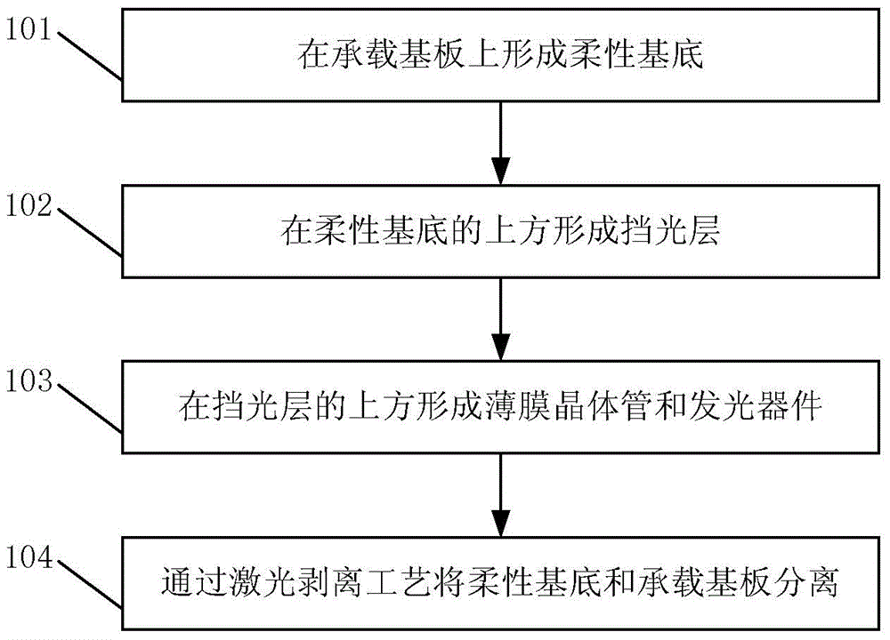
[0030] In order for those skilled in the art to better understand the technical solution of the present invention, the flexible display substrate provided by the present invention, its manufacturing method, and the flexible display device are described in detail below with reference to the accompanying drawings.

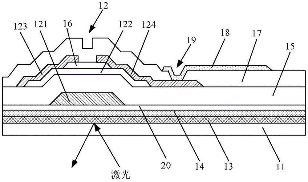
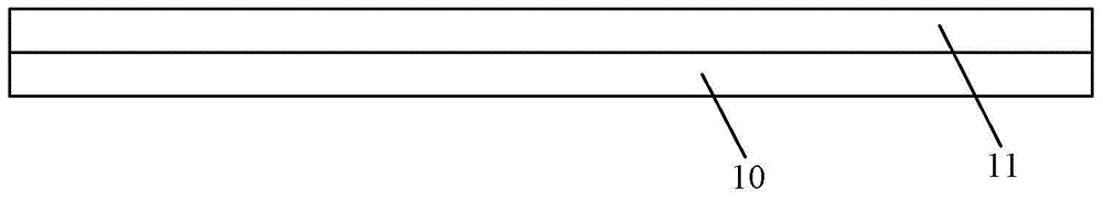
[0031] figure 1 A schematic structural diagram of a flexible display substrate provided in Embodiment 1 of the present invention, as shown in figure 1 As shown, the flexible display substrate includes: a flexible substrate 11, a thin film transistor 12 and a light emitting device are formed on the flexible substrate 11, a light blocking layer 13 is formed between the flexible substrate 11 and the thin film transistor 12, and the light blocking layer 13 is used to block Laser light irradiated from the flexible substrate 11 side.

[0032] Preferably, the material of the flexible substrate may include: polyimide (PI), polyethylene naphthalate (PEN) or polyethylene tere...


PUM


Abstract

The invention discloses a flexible display substrate, a manufacturing method thereof, and a flexible display device. The flexible display substrate includes: a flexible substrate, a thin film transistor and a light emitting device are formed on the flexible substrate, a light blocking layer is formed between the flexible substrate and the thin film transistor, and the light blocking layer is used to block the Laser light irradiated on one side of the flexible substrate. In the flexible display substrate and its manufacturing method and the technical solution of the flexible display device provided by the present invention, a light-blocking layer is formed between the flexible substrate and the thin film transistor, and the light-blocking layer can block the laser light irradiated from the side of the flexible substrate, avoiding the The laser causes damage to the thin film transistor, thereby avoiding the threshold voltage drift of the thin film transistor and the failure of the characteristics of the thin film transistor, thereby avoiding the problem that the display effect of the flexible display substrate decreases or even cannot be displayed normally after laser stripping.

Description

technical field [0001] The invention relates to the field of display technology, in particular to a flexible display substrate, a manufacturing method thereof, and a flexible display device. Background technique [0002] The flexible display device has the advantages of being convenient to carry and being bendable and curlable, so it has become a research and development hotspot in current display technology. [0003] In the prior art, the manufacturing method of a flexible display substrate generally includes: coating a flexible substrate on a carrier substrate, and preparing a thin film transistor (Thin Film Transistor, TFT for short) and an organic light-emitting diode (Organic Light-Emitting Diode) on the flexible substrate. , referred to as: OLED) to form a flexible display substrate, after the preparation is completed, the fabricated flexible display substrate is peeled off from the carrier substrate. Laser lift-off is a commonly used flexible display substrate lift-o...

Claims


Application Information

Patent Timeline
Patent Type & Authority Patents(China)
IPC IPC(8): H01L51/52H01L51/56H01L27/32
Inventor 李旭远姜春生
Owner BOE TECH GRP CO LTD
Why Eureka
Try Eureka