Polysilicon thin film transistor and manufacturing method thereof

A polysilicon thin film and manufacturing method technology, used in transistors, semiconductor/solid-state device manufacturing, semiconductor devices, etc., can solve the problems of source and drain punch-through, loss of transistor characteristics, etc., to prevent source-drain punch-through, improve characteristics, and avoid threshold voltage. Drift effect

Active Publication Date: 2021-03-19
SHANGHAI HUAHONG GRACE SEMICON MFG CORP
View PDF5 Cites 0 Cited by
  • Summary
  • Abstract
  • Description
  • Claims
  • Application Information

AI Technical Summary

Problems solved by technology

Both single crystal silicon thin film transistors and polycrystalline silicon thin film transistors need ion implantation doping in the process of forming source and drain electrodes. Because the implanted ions diffuse more easily in polycrystalline silicon than in single crystal silicon, polycrystalline silicon thin film transistors and single crystal Compared with silicon thin film transistors, the channel length is narrower, and it is easy to cause source and drain punchthrough due to the overlapping of source and drain depletion regions, which may lead to the loss of transistor characteristics.

Method used


Image

  • Polysilicon thin film transistor and manufacturing method thereof
  • Polysilicon thin film transistor and manufacturing method thereof
  • Polysilicon thin film transistor and manufacturing method thereof

Examples


Embodiment Construction

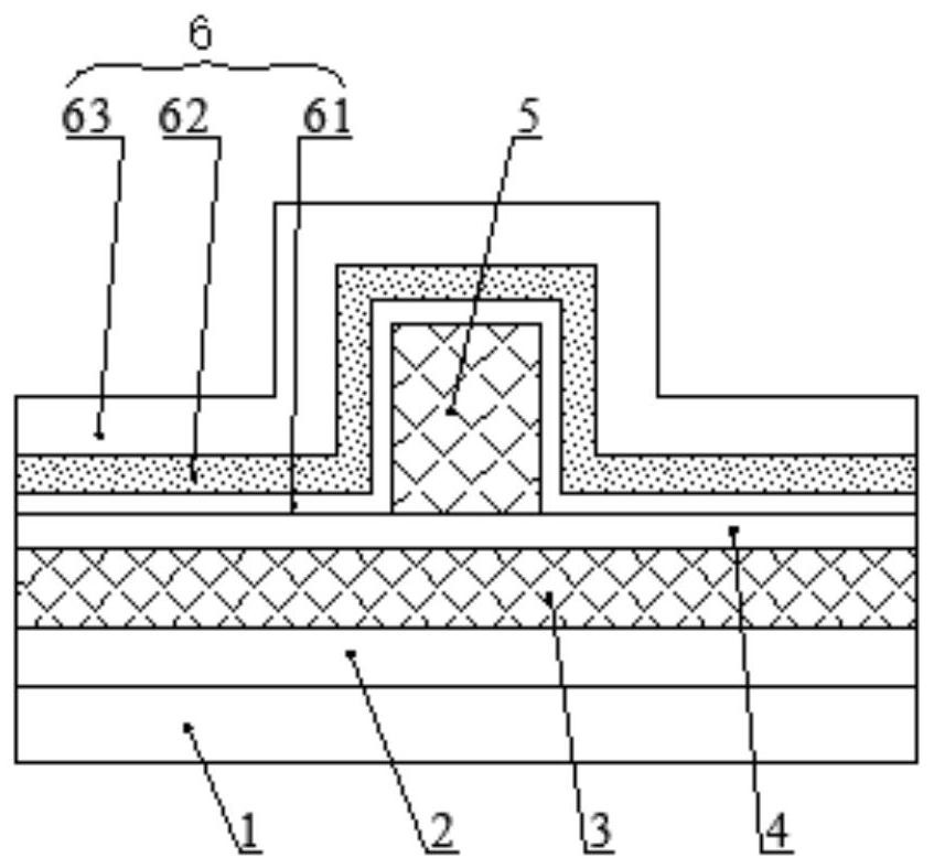
[0031] The inventor found that the channel length of polysilicon thin film transistors tends to be narrower compared with single crystal silicon thin film transistors. In order to solve the problem of narrowing the channel length of polysilicon thin film transistors, the inventors tried to reduce the dose of light doping by ion implantation , but it is found that since the gate, source and drain of the polysilicon thin film transistor are implanted with ions at the same time, if the dose of lightly doped ion implantation in the source and drain regions is reduced, the dose of lightly doped ion implanted in the gate will also be reduced, so First, it will cause the threshold voltage of the thin film transistor to drift.

[0032] In the embodiment of the present invention, the first ion implantation process is performed to implant ions into the polysilicon gate layer; the second ion implantation process is performed to inject ions into the polysilicon gate layer and the polysilic...


PUM

PropertyMeasurementUnit
thicknessaaaaaaaaaa

Abstract

The invention provides a polysilicon thin film transistor and a manufacturing method thereof. The manufacturing method comprises the steps of: providing a substrate, forming a polysilicon active layeron the substrate, sequentially forming a gate insulating layer and a polysilicon gate layer on the polysilicon active layer; performing a chemico-mechanical polishing process for removing a part of asidewall covering layer above the polysilicon gate layer; and performing a first ion implantation process to implant ions into the polysilicon gate layer; performing a second ion implantation processto implant ions into the polysilicon gate layer and polysilicon active layer on both sides of the sidewall, so as to form a source doped region and a drain doped region. Under the condition that theion implantation dose of the polysilicon gate layer is not reduced, the source-drain depletion region overlap is reduced by reducing the ion implantation doses of the source doped region and the draindoped region, thereby preventing source and drain penetration. At the same time, the ion implantation dose of the polysilicon gate layer is ensured, the threshold voltage drift of the thin film transistor is avoided, and the characteristics of the polysilicon thin film transistor are improved.

Description

technical field [0001] The invention relates to the technical field of semiconductor integrated circuits, in particular to a polysilicon thin film transistor and a manufacturing method thereof. Background technique [0002] The source and drain of the polysilicon thin film transistor are formed on the polysilicon active layer, and because of its high mobility, it is more and more used. The source and drain of the single crystal silicon thin film transistor are formed on the single crystal silicon active layer. Both single crystal silicon thin film transistors and polycrystalline silicon thin film transistors need ion implantation doping in the process of forming source and drain electrodes. Because the implanted ions diffuse more easily in polycrystalline silicon than in single crystal silicon, polycrystalline silicon thin film transistors and single crystal Compared with silicon thin film transistors, the channel length is narrower, and it is easy to cause source and drain...

Claims


Application Information

Patent Timeline
Patent Type & Authority Patents(China)
IPC IPC(8): H01L21/265H01L21/336H01L29/06H01L29/08H01L29/423H01L29/786
Inventor 沈思杰
Owner SHANGHAI HUAHONG GRACE SEMICON MFG CORP
Why Eureka
Try Eureka