3d NAND flash memory and its preparation method

A flash memory and suppression layer technology, applied in semiconductor devices, electrical components, circuits, etc., can solve the problems of dielectric layer breakdown between adjacent gate layers, gate layer threshold voltage drift, and storage layer charge loss, etc. The effect of reducing threshold voltage drift, reducing leakage, and ensuring stability

Active Publication Date: 2020-08-14
YANGTZE MEMORY TECH CO LTD
View PDF8 Cites 0 Cited by
  • Summary
  • Abstract
  • Description
  • Claims
  • Application Information

AI Technical Summary

Problems solved by technology

[0005] In view of the above-mentioned shortcomings of the prior art, the purpose of the present invention is to provide a 3D NAND flash memory and its preparation method, which are used to solve the problem that the 3D NAND flash memory in the prior art is easily caused by the reduction of the thickness of the inter-gate dielectric layer. Leakage between gate layers may even cause the breakdown of the inter-gate dielectric layer between adjacent gate layers. In 3D NAND flash memory, inter-layer coupling interference between adjacent gate layers may cause gate layer The problem of threshold voltage drift in 3D NAND flash memory, and the lateral loss of charge in the storage layer in 3D NAND flash memory, resulting in the problem of threshold voltage drift of the gate layer

Method used


Image

  • 3d NAND flash memory and its preparation method
  • 3d NAND flash memory and its preparation method
  • 3d NAND flash memory and its preparation method

Examples


Embodiment 1

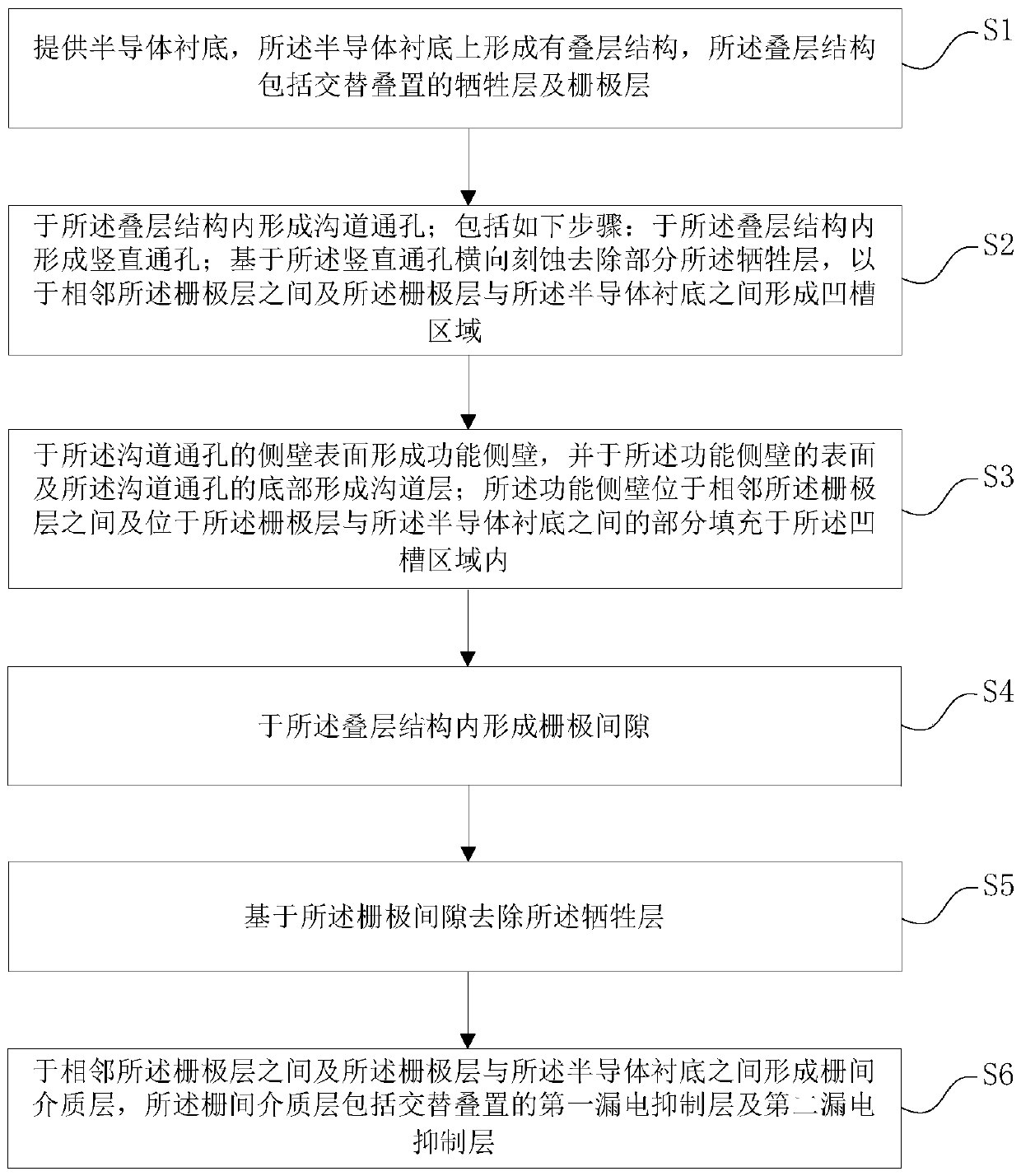
[0098] see figure 1 , the present embodiment also provides a method for preparing a 3D NAND flash memory, the method for preparing the 3D NAND flash memory includes the following steps:

[0099] 1) providing a semiconductor substrate, on which a stacked structure is formed, and the stacked structure includes alternately stacked sacrificial layers and gate layers;

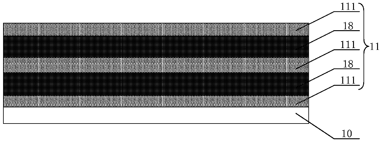
[0100] 2) Forming a channel via hole in the stacked structure; including the following steps: forming a vertical via hole in the stacked structure; laterally etching and removing part of the sacrificial layer based on the vertical via hole, to forming a groove region between adjacent gate layers and between the gate layer and the semiconductor substrate;

[0101] 3) forming a functional sidewall on the surface of the sidewall of the channel through hole, and forming a channel layer on the surface of the functional sidewall and the bottom of the channel through hole; The portion between the gate layer and between t...

Embodiment 2

[0174] read on Figure 23 and Figure 25 , this embodiment also provides a 3D NAND flash memory, the 3D NAND flash memory includes: a semiconductor substrate 10; a stacked structure 31, the stacked structure 31 is located on the semiconductor substrate 10, the stacked structure 31 includes alternately stacked inter-gate dielectric layers 17 and gate layers 18; the inter-gate dielectric layer 17 includes air gaps 173 and alternately stacked first leakage suppression layers 171 and second leakage suppression layers 172, the air The gap 173 is located in the structure in which the first leakage suppression layer 171 and the second leakage suppression layer 172 are alternately stacked; the channel via hole 12, and the channel via hole 12 is located in the stacked structure 31; The channel via hole 12 includes several groove regions 122, and the groove region 122 is located between adjacent gate layers 18 and between the gate layer 18 and the semiconductor substrate 10; the functi...


PUM


Abstract

The invention provides a 3D NAND flash memory and a preparation method thereof, comprising the following steps: providing a semiconductor substrate, on which a stacked structure is formed, including alternately stacked sacrificial layers and gate layers; forming a trench in the stacked structure The channel via hole; the channel via hole includes several groove regions between adjacent gate layers and between the gate layer and the semiconductor substrate; the functional sidewall is formed on the side wall surface of the channel via hole, and The surface of the functional sidewall and the bottom of the channel via hole form a channel layer; form a gate gap in the stack structure; remove the sacrificial layer based on the gate gap; between adjacent gate layers and between the gate layer and the semiconductor substrate An inter-gate dielectric layer is formed between the bottom, and the inter-gate dielectric layer includes alternately stacked first leakage suppression layers and second leakage suppression layers. The invention can effectively reduce the electric leakage between the adjacent gate layers, improve the breakdown resistance of the inter-gate dielectric layer between the adjacent gate layers, and reduce the coupling effect between the adjacent gate layers.

Description

technical field [0001] The invention belongs to the technical field of integrated circuit design and manufacture, and in particular relates to a 3D NAND flash memory and a preparation method. Background technique [0002] In recent years, the development of flash memory (Flash Memory) has been particularly rapid. The main feature of flash memory is that it can keep stored information for a long time without power on, and it has high integration, fast access speed, easy erasing and resetting. It has the advantages of writing and so on, so it has been widely used in many fields such as microcomputer and automatic control. In order to further increase the bit density (Bit Density) of the flash memory while reducing the bit cost (Bit Cost), three-dimensional flash memory (3D NAND) technology has been developed rapidly. [0003] The stack structure of the existing 3D NAND flash memory is formed by alternately stacking multiple gate layers (ie gate word line layers) and inter-gat...

Claims


Application Information

Patent Timeline
Patent Type & Authority Patents(China)
IPC IPC(8): H01L27/11551H01L27/11578
CPCH10B41/20H10B43/20
Inventor 肖莉红
Owner YANGTZE MEMORY TECH CO LTD
Why Eureka
Try Eureka