PCB (Printed Circuit Board) automatic detector

A technology for PCB boards and inspection machines, which can be used in measurement devices, optical testing of flaws/defects, and material analysis by optical means, which can solve the problems of low efficiency and low scanning image quality.

Active Publication Date: 2017-09-26
深圳宜美智科技股份有限公司
View PDF7 Cites 2 Cited by
  • Summary
  • Abstract
  • Description
  • Claims
  • Application Information

AI Technical Summary

Problems solved by technology

[0005] The embodiment of the present invention provides a PCB board automatic inspection machine with high defect detection efficiency and scanning imaging quality for P...

Method used


Image

  • PCB (Printed Circuit Board) automatic detector
  • PCB (Printed Circuit Board) automatic detector
  • PCB (Printed Circuit Board) automatic detector

Examples


Embodiment Construction

[0090] Please refer to the drawings, in which the same component symbols represent the same components, and the principle of the present invention is exemplified by being implemented in a suitable computing environment. The following description is based on the illustrated specific embodiments of the present invention, which should not be regarded as limiting other specific embodiments of the present invention that are not described in detail herein.

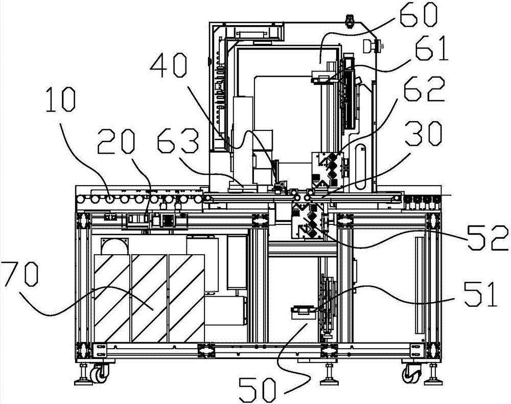
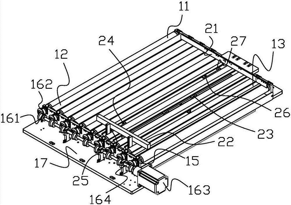
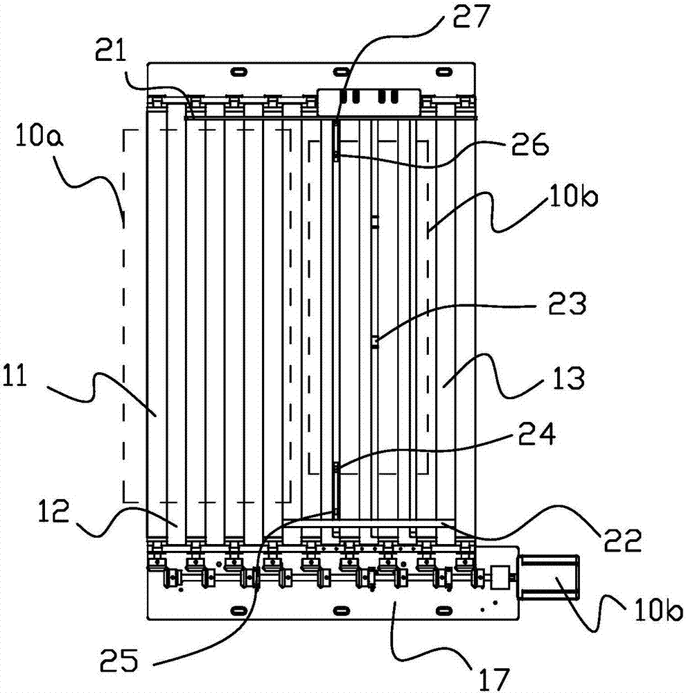
[0091] Please refer to figure 1 , figure 1 It is a schematic front view of the preferred embodiment of the PCB board automatic inspection machine of the present invention. The preferred embodiment of the PCB board automatic inspection machine of the present invention includes a transmission device having a feeding position 10a, a first correction position 10b, a second correction position 20c, a first detection position 20d and a second detection position 20e, and a first correction mechanism 20. The second calibration mechanism 40...


PUM


Abstract

The invention provides a PCB (Printed Circuit Board) automatic detector. The PCB automatic detector comprises a transmission device, a first correcting mechanism and an image acquiring device, wherein the transmission device comprises a charging position for introducing a PCB to be detected, a first correcting position for initially correcting the PCB to be detected, and a detection position for acquiring an image of the PCB to be detected; the transmission device is used for transmitting the PCB to be detected to the first correcting position and the detection position in sequence from the charging position; the first correcting mechanism is used for correcting the PCB positioned at the first correction position; the image acquiring device is used for acquiring the image of the PCB positioned at the detection position. By adopting the PCB automatic detector, the first correcting mechanism is arranged, so that the transmission accuracy is increased; the transmission device is arranged, so that the transmission stability is improved; the image acquiring device is arranged, so that the detection efficiency is increased.

Description

Technical field [0001] The invention relates to the field of circuit board circuit detection, in particular to a PCB board automatic detection machine. Background technique [0002] With the development of science and technology, manufacturers have higher and higher requirements for the detection of PCB boards (printed circuit boards), such as the efficiency of PCB board defect detection and the imaging quality of defect scanning. [0003] In the existing PCB board automatic inspection machine, either the inspection efficiency or the imaging quality of the defect scanning is emphasized. For example, the traditional AOI inspection machine has low recognition after imaging and is more likely to cause misjudgment; such as the existing The PCB board inspection machine can only inspect one side of the PCB board at the same time, which is a waste of inspection time; or, for example, the transmission mechanism of the existing PCB board inspection machine is easy to slip and the conveyed o...

Claims


Application Information

Patent Timeline
IPC IPC(8): G01N21/89
CPCG01N21/8914Y02W30/82
Inventor 陈胜鹏
Owner 深圳宜美智科技股份有限公司
Why Eureka
Try Eureka