Display screen manufacturing method and display screen
A manufacturing method and a technology of a display screen, applied in the field of display screens, can solve the problem that the screen-to-body ratio of mobile terminals cannot be further improved
- Summary
- Abstract
- Description
- Claims
- Application Information
AI Technical Summary
Problems solved by technology
Method used
Image
Examples
Embodiment 1
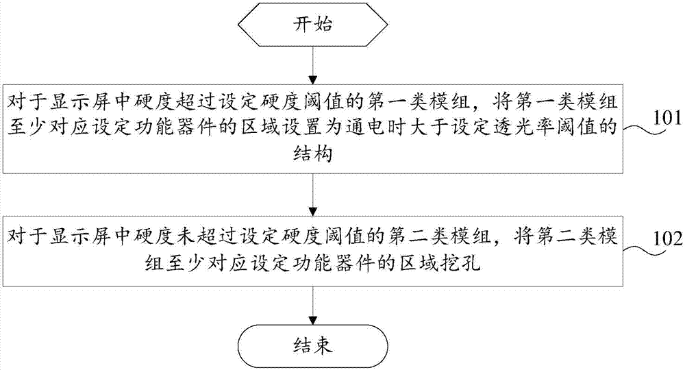
[0037] refer to figure 1 , which shows a flow chart of the display screen manufacturing method according to Embodiment 1 of the present invention, which may specifically include the following steps:
[0038] Step 101, for the first type of modules in the display screen whose hardness exceeds the set hardness threshold, set at least the area of the first type module corresponding to the set functional device to a structure that is greater than the set light transmittance threshold when powered on.
[0039] In the embodiment of the present invention, in order to increase the screen-to-body ratio of the mobile terminal, the original display screen design can be improved, that is, a part of the functional devices originally arranged at the top of the display screen can be transferred to the bottom of the display screen, so that the entire The screen can be used for display. However, for the functional devices transferred to the bottom of the display screen, it is also necessary...
Embodiment 2
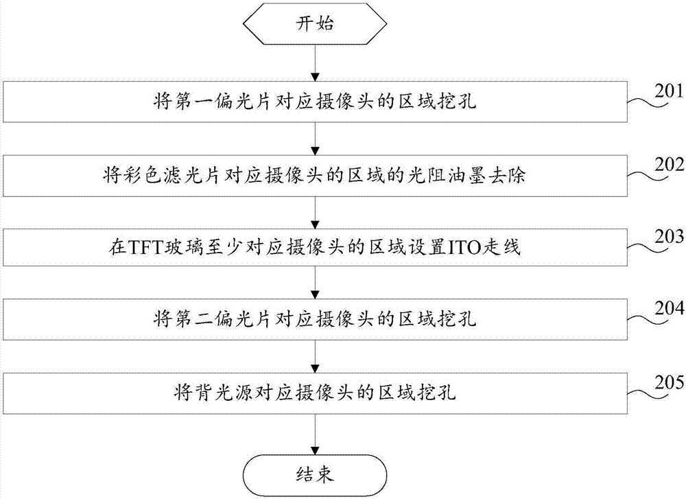
[0046] refer to Figure 2A , showing a flow chart of the method for manufacturing a display screen according to Embodiment 2 of the present invention, wherein the display screen may be a TFT display screen, and the first type of module may include a cover glass, a color filter, a liquid crystal layer, and a TFT glass, The second type of module may include a first polarizer, a second polarizer and a backlight, and the setting function device may be a camera, which may specifically include the following steps:
[0047] Step 201, digging a hole in the area of the first polarizer corresponding to the camera.
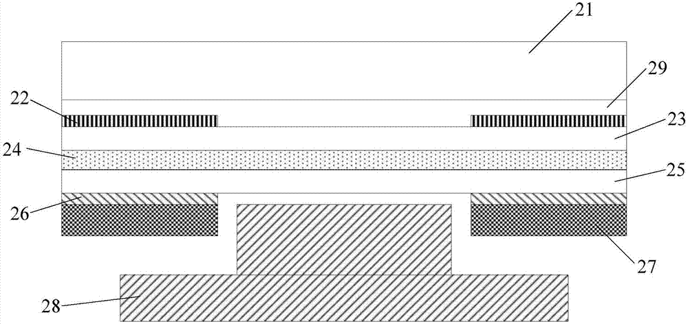
[0048] refer to Figure 2B , shows a schematic structural view of the TFT display screen of the present invention. like Figure 2B As shown, the cover glass 21 is located on the outermost surface of the display screen, the first polarizer 22 is located below the cover glass 21, and the gap is filled with OCA (Optically Clear Adhesive, optically transparent adhesive) opt...
Embodiment 3
[0073] refer to Figure 3A , shows a flow chart of the display screen manufacturing method according to Embodiment 3 of the present invention, wherein the display screen may be an AMOLED display screen, the first type of module may include cover glass, Encap glass and LTPS glass, and the second type of module It can include polarizers, LTPS glass protective film and foam protective layer, and the setting function device can be a camera. Specifically, it can include the following steps:
[0074] Step 301, digging holes in the area of the polarizer corresponding to the camera.
[0075] refer to Figure 3B , shows a schematic structural view of the AMOLED display screen of the present invention. like Figure 3B As shown, the cover glass 31 is located on the outermost surface of the display screen, the polarizer 32 is located under the cover glass 31, and the gap between the two is filled with OCA optical glue 38, and the bottom of the polarizer 32 is Encap glass 33 and LTPS ...
PUM
 Abstract
Description
Claims
Application Information


