Preparation method of chip packaging module set and packaging structure
A chip packaging and chip technology, which is applied in the field of chip packaging module preparation method and packaging structure, can solve the problems of complex process and high technical difficulty of chip packaging technology, and achieve the effect of reducing packaging cost, simplifying process flow and technical difficulty
- Summary
- Abstract
- Description
- Claims
- Application Information
AI Technical Summary
Problems solved by technology
Method used
Image
Examples
Embodiment 1
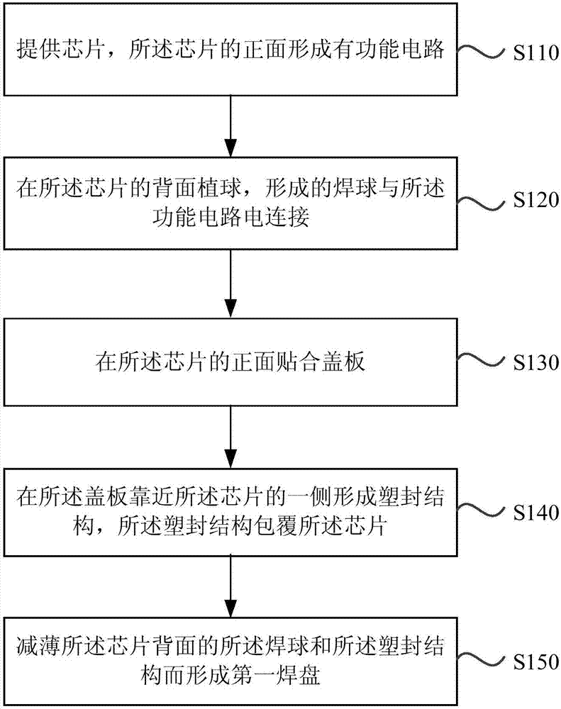
[0042] Figure 2A It is a flowchart of a method for preparing a chip packaging module provided in Embodiment 1 of the present invention, Figure 2B-Figure 2F It is a chip packaging module formed in each step of the chip packaging module manufacturing method provided in Embodiment 1 of the present invention. This embodiment is applicable to the case where the surface of the chip in the chip packaging structure is exposed, and specifically includes the following steps:
[0043] Step 110, providing a chip, and a functional circuit is formed on the front side of the chip;
[0044] see Figure 2B , a chip 210 is provided, the front side 211 of the chip 210 is formed with functional circuits.
[0045] Step 120, planting balls on the back of the chip, and the formed solder balls are electrically connected to the functional circuit;
[0046] see Figure 2C , planting balls on the back side 212 of the chip 210 to form solder balls 281, the solder balls 281 are electrically connect...
Embodiment 2
[0069] Figure 3A It is a flow chart of a method for preparing a chip packaging module provided in Embodiment 2 of the present invention; Figure 3B-Figure 3F It is a chip packaging module formed in each step of the chip packaging module manufacturing method provided in Embodiment 2 of the present invention. On the basis of the foregoing examples, optimization is carried out, and the preparation method comprises:
[0070] Step 210, providing a chip, the front side of the chip is formed with a functional circuit;
[0071] see Figure 3B , a chip 310 is provided, the front side 311 of which is formed with functional circuits.
[0072] Step 220, planting balls on the back of the chip, and the formed solder balls are electrically connected to the functional circuit;
[0073] see Figure 3C , planting balls on the back surface 312 of the chip 310 to form solder balls 381 , the solder balls 381 are electrically connected to the functional circuit, specifically, the solder ball ...
Embodiment 3
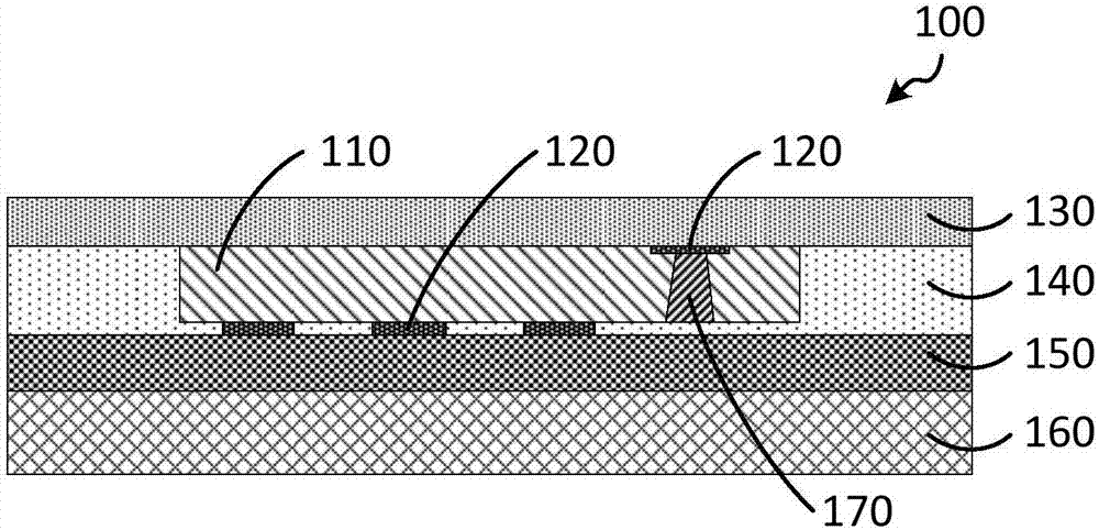
[0086] Figure 4 A schematic cross-sectional view of a chip packaging module provided in Embodiment 3 of the present invention. This embodiment is applicable to the situation where the surface of the chip is exposed. The specific structure of the chip packaging module 400 is as follows:
[0087] A chip 410, the front 411 of the chip 410 is provided with a functional circuit; the back 412 of the chip 410 is provided with solder balls, and the solder balls are electrically connected to the functional circuit;
[0088] a cover plate 430 attached to the front surface 411 of the chip 410;
[0089] The plastic encapsulation structure 440 is located on the side of the cover plate 430 close to the chip 410 and covers the chip 410;
[0090] The first pad 480 , the first pad 480 is a cross section of the solder ball formed by thinning the plastic package structure 440 and the solder ball, and the package structure exposes the first pad 480 .
[0091] The PCB board 460 , the PCB board ...
PUM
 Abstract
Description
Claims
Application Information
 - R&D
- Intellectual Property
- Life Sciences
- Materials
- Tech Scout
- Unparalleled Data Quality
- Higher Quality Content
- 60% Fewer Hallucinations
Browse by: Latest US Patents, China's latest patents, Technical Efficacy Thesaurus, Application Domain, Technology Topic, Popular Technical Reports.
© 2025 PatSnap. All rights reserved.Legal|Privacy policy|Modern Slavery Act Transparency Statement|Sitemap|About US| Contact US: help@patsnap.com


