Three-dimensional board-level fan-out type packaging structure and manufacturing method thereof

A packaging structure and manufacturing method technology, which is applied in semiconductor/solid-state device manufacturing, electrical components, electric solid-state devices, etc., can solve problems such as inability to meet multi-functional and other application requirements, high processing costs of packaging structures, and unstable dimensions. Achieve the effect of improving area utilization, low cost, offsetting bending and dimensional instability

Pending Publication Date: 2022-02-08
HUATIAN TECH KUNSHAN ELECTRONICS
View PDF0 Cites 0 Cited by
  • Summary
  • Abstract
  • Description
  • Claims
  • Application Information

AI Technical Summary

Problems solved by technology

The existing packaging structure has high processing costs and cannot meet the multi-functional and other application requ

Method used


Image

  • Three-dimensional board-level fan-out type packaging structure and manufacturing method thereof
  • Three-dimensional board-level fan-out type packaging structure and manufacturing method thereof
  • Three-dimensional board-level fan-out type packaging structure and manufacturing method thereof

Examples


Embodiment Construction

[0041] The preferred embodiments of the present invention will be described in detail below in conjunction with the accompanying drawings, so that the advantages and features of the present invention can be more easily understood by those skilled in the art, so as to define the protection scope of the present invention more clearly.

[0042] like Figure 1 to Figure 10 A preferred embodiment of the manufacturing method of a three-dimensional board-level fan-out packaging structure shown, which includes the following steps:

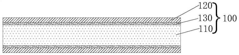
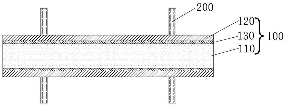
[0043] S1, take a carrier sheet 110, apply an adhesive on the front and back of the carrier sheet 110 respectively to form an adhesive layer 130; then bond the copper foil 120 to the adhesive layer 130 to form a composite carrier 100; The material of the carrier sheet 110 can be one of silicon, glass, metal or organic material or a combination of multiple materials; in this embodiment, the carrier sheet 110 is preferably made of silicon;

[0044] S2, maki...


PUM


Abstract

The invention discloses a three-dimensional board-level fan-out type packaging structure and a manufacturing method thereof. The manufacturing method comprises the steps of respectively bonding copper foils on the front surface and the back surface of a carrier piece, and forming a composite carrier plate; manufacturing a conductive structure on the composite carrier plate; manufacturing conductive salient points on a bonding pad of a chip I; mounting the chip I on the composite carrier plate; forming a plastic package layer wrapping the conductive structure and the chip I on the composite carrier plate; respectively manufacturing a rewiring layer and an insulating dielectric layer on the surface of the plastic package layer; removing the carrier piece to obtain a packaged semi-finished product structure; respectively manufacturing a rewiring layer and an insulating dielectric layer on the back surface of the chip I for packaging the semi-finished product structure; manufacturing a signal leading-out structure and an electric connection structure on the packaged semi-finished product structure; and inversely mounting a chip II on the electric connection structure, and wrapping the chip II with an outer plastic package protection layer to obtain the three-dimensional board-level fan-out type packaging structure. According to the invention, the warping problem caused by processing can be effectively improved, multifunctional integration can be realized, and the processing cost can be reduced.

Description

technical field [0001] The invention relates to the technical field of semiconductor chip packaging, in particular to a three-dimensional board-level fan-out packaging structure and a manufacturing method thereof. Background technique [0002] With the increasingly stringent requirements for portable and multi-functional consumer electronic products, integrating more functions, improving product performance, thinning and reducing manufacturing costs have gradually become the development direction of intelligent terminal products and industry manufacturers. As a kind of wafer-level packaging, the fan-out packaging structure greatly increases the number of package I / Os, which is in line with the development direction of multi-functional chips. However, due to its high processing cost, it is not suitable for large-scale production has certain obstacles. [0003] Therefore, it is necessary to propose a device that can accommodate more I / Os, reduce chip size and thickness, integ...

Claims


Application Information

Patent Timeline
IPC IPC(8): H01L21/60H01L21/56H01L23/31H01L23/498H01L25/04
CPCH01L24/02H01L24/81H01L21/568H01L23/3107H01L23/49838H01L25/04H01L2224/02379H01L2224/02381H01L2224/81191
Inventor 马书英肖智轶常笑男吴阿妹
Owner HUATIAN TECH KUNSHAN ELECTRONICS
Why Eureka
Try Eureka