Production method for digital isolation core packaging piece

A digital isolation and production method technology, applied in the direction of electrical components, semiconductor devices, electric solid devices, etc., can solve the problems of unreachable interface delamination, low packaging yield rate required by standards, etc., and achieve weight reduction, high reliability isolation circuits, Effect of High Communication Rate

Active Publication Date: 2020-02-11
TIANSHUI HUATIAN TECH
View PDF5 Cites 0 Cited by
  • Summary
  • Abstract
  • Description
  • Claims
  • Application Information

AI Technical Summary

Problems solved by technology

[0003] The purpose of the present invention is to provide a method for producing high-reliability high-voltage isolation functional plastic packages, so as to solve the problem that the interfac

Method used


Image

  • Production method for digital isolation core packaging piece
  • Production method for digital isolation core packaging piece
  • Production method for digital isolation core packaging piece

Examples


Example Embodiment

[0040] Example 1

[0041] A wire frame body with a length of 269.6 mm and a width of 83.0 mm was fabricated. 112 packaging units were arranged on the lead frame body, and all the packaging units were arranged in a matrix of 7 rows and 16 columns. Improve material utilization and production efficiency.

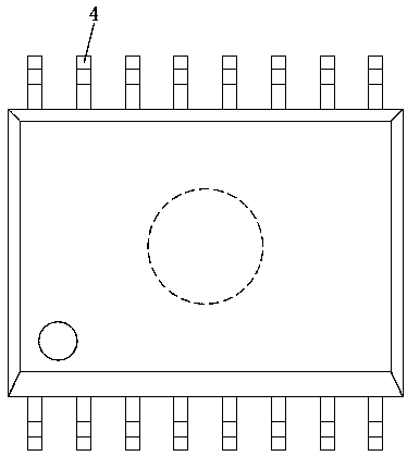
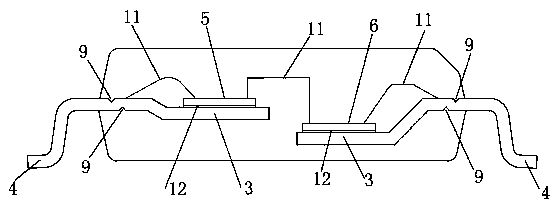
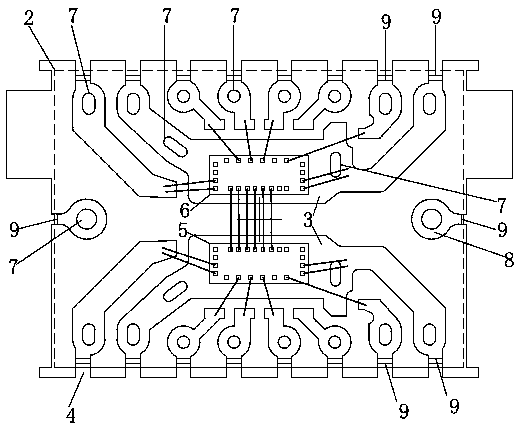
[0042] The packaging unit 2 includes two carriers 3 to realize multi-chip integrated packaging; the carriers 3 are arranged oppositely, the height difference between the carriers 3 is equal to 0, the separation distance between the two carriers 3 is equal to 0.8mm, and 16 are arranged along the non-opposite periphery of the carrier 3. Radial pins 4 are arranged on the two long sides of the package unit 2, a pair of symmetrical lugs 8 are arranged on the center axis of the two carriers 3; n process holes 7 are arranged on the periphery of the carrier 3, depending on the size of the chip . Each pin 4 is provided with a process hole 7 and a plurality of asymmetrical V-shaped transver...

Example Embodiment

[0055] Example 2

[0056] A wire frame body with a length of 269mm and a width of 83mm is fabricated. 112 packaging units are arranged on the lead frame body, and all the packaging units are arranged in a matrix of 7 rows and 16 columns. The package unit 2 includes two carriers 3 arranged oppositely, the height difference between the carriers 3 is equal to 0.50mm, the separation distance between the two carriers 3 is equal to 0.8mm, and 16 radial pins are arranged along the non-opposite periphery of the carrier 3 A pair of symmetrical lugs 8 are provided on the two long sides of the package unit 2 in four rows, and the center axis of the two carriers 3 spaced apart; n process holes 7 are provided on the periphery of the carrier 3, and a process hole is provided on each pin 4 7 and the front and back sides are provided with a plurality of asymmetrical V-shaped transverse grooves 9; at least one end of the non-opposing periphery of the carrier 3 is connected with at least one pin 4...

Example Embodiment

[0068] Example 3

[0069] A wire frame body with a length L of 300 mm and a width of 100 mm is fabricated. 112 packaging units are arranged on the lead frame body, and all the packaging units are arranged in a matrix of 7 rows and 16 columns. The package unit 2 includes two carriers 3 arranged oppositely, the height difference between the carriers 3 is equal to 0, the separation distance between the two carriers 3 is equal to 0.3mm, and 16 radial pins 4 are arranged along the non-opposite periphery of the carrier 3 A pair of symmetrical lugs 8 are arranged on the two long sides of the package unit 2 separated by the two carriers 3; there are n process holes 7 on the periphery of the carrier 3, and a process hole 7 is provided on each pin 4 A plurality of asymmetrical V-shaped transverse grooves 9 are provided on the front and back sides; at least one end of the non-opposing periphery of the carrier 3 is connected with at least one pin 4.

[0070] The production process is as follo...


PUM

PropertyMeasurementUnit
Separation distanceaaaaaaaaaa
Lengthaaaaaaaaaa
Widthaaaaaaaaaa

Abstract

The invention discloses a production method for a digital isolation core packaging part, which belong to the field of microelectronic assembly and packaging and aims to solve the problems that the interface layering of pins, carriers and plastic packaging materials of an integrated circuit packaged by an existing method cannot meet the standard requirement and the packaging yield is low. The production method for the digital isolation core packaging piece comprises the following steps of: A, thinning and scribing a wafer to form a lead frame, B, adhering a chip to a carrier of the lead frame,C, baking, D, conducting plasma cleaning after baking, E, conducting pressure welding, and F, performing plastic packaging, printing and testing by adopting a packaging production process, and then performing rib cutting and one-step molding to obtain the wide-body small-shape packaging piece. The high-efficiency production method provided by the invention can be used for producing a digital IC packaging piece with the reliability reaching the high-voltage isolation function on the MSL3.

Description

technical field [0001] The invention belongs to the field of microelectronic assembly and packaging, and in particular relates to a production method of a digital isolation core package. Background technique [0002] With the advancement of Industry 4.0 and the popularization of smart manufacturing, more reliable sensors, controllers and actuators are required in industrial systems, and these systems need to be escorted by isolation technology. Isolation is a means of transferring data and power between high-voltage and low-voltage circuits while preventing dangerous DC or uncontrolled transient currents from flowing between the two. Compared with traditional optocouplers, digital isolation chips can achieve lower cost, smaller size, high isolation withstand voltage, wide temperature range, high integration performance, low power consumption and more reliable isolation circuits, and have high communication rates and long life . The rapid growth of emerging fields such as e...

Claims


Application Information

Patent Timeline
IPC IPC(8): H01L21/56H01L21/60H01L23/62
CPCH01L21/56H01L24/83H01L23/62H01L2224/83203H01L2224/73265H01L2224/48247H01L2224/48137H01L2224/97H01L2224/49175H01L2224/32245H01L2924/00012
Inventor 张易勒李习周蔺兴江赵萍李琦
Owner TIANSHUI HUATIAN TECH
Why Eureka
Try Eureka