Same-side electrode InGaAs backlight monitoring detector and manufacturing method thereof

A manufacturing method and detector technology, applied in the field of optical communication, can solve the problems of increased material cost, fragmentation risk, poor adhesion between metal and InP substrate, etc., and achieve the effect of saving packaging cost and low fragmentation risk.

Pending Publication Date: 2022-06-24
FUJIAN Z K LITECORE LTD
View PDF0 Cites 0 Cited by
  • Summary
  • Abstract
  • Description
  • Claims
  • Application Information

AI Technical Summary

Problems solved by technology

The disadvantages of the existing structure are: 1) Due to the different-surface electrode configuration, it needs to be used with spacers in the actual use process, which not only increases the material cost but also increases the die-bonding steps and reduces the production capacity; 2) The entire wafer is shared N-type electrode, the chip cannot identify abnormal N-type ohmic contact core particles

Method used


Image

  • Same-side electrode InGaAs backlight monitoring detector and manufacturing method thereof
  • Same-side electrode InGaAs backlight monitoring detector and manufacturing method thereof
  • Same-side electrode InGaAs backlight monitoring detector and manufacturing method thereof

Examples


Embodiment Construction

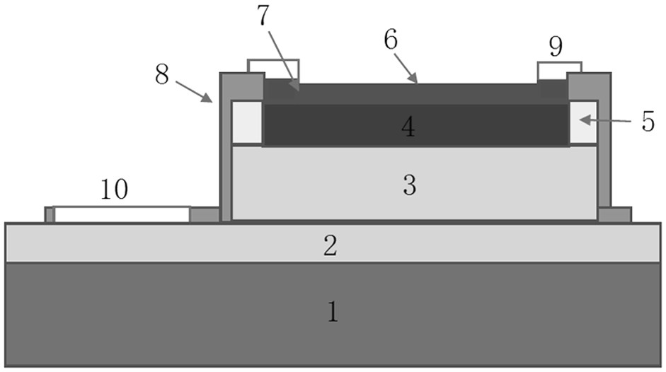
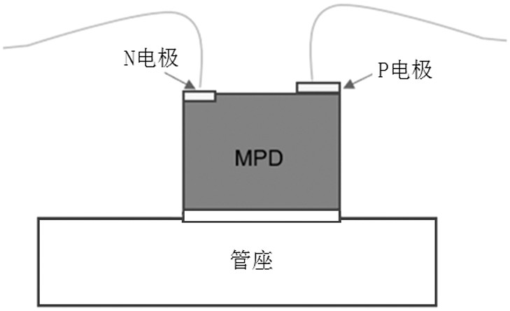
[0026] The present invention will be further described below with reference to the accompanying drawings and embodiments.

[0027] It should be noted that the following detailed description is exemplary and intended to provide further explanation of the application. Unless otherwise defined, all technical and scientific terms used herein have the same meaning as commonly understood by one of ordinary skill in the art to which this application belongs.

[0028] It should be noted that the terminology used herein is for the purpose of describing specific embodiments only, and is not intended to limit the exemplary embodiments according to the present application. As used herein, unless the context clearly dictates otherwise, the singular is intended to include the plural as well, furthermore, it is to be understood that when the terms "comprising" and / or "including" are used in this specification, it indicates that There are features, steps, operations, devices, components and / ...


PUM

PropertyMeasurementUnit
Thicknessaaaaaaaaaa

Abstract

The invention relates to a same-side electrode InGaAs backlight monitoring detector and a manufacturing method thereof.The detector comprises an InP substrate, an N-type InP layer is arranged on the InP substrate, an unintentionally-doped intrinsic I-InGaAs layer is arranged in a first area on the N-type InP layer, an N electrode is arranged in a second area on the N-type InP layer, an InP window layer is arranged on the I-InGaAs layer, a Zn diffusion area is formed in a photosensitive area of the InP window layer by means of Zn diffusion doping, and the N electrode is arranged on the first area of the N-type InP layer. The other part is an unintentionally doped U-InP region, the upper middle part of the Zn diffusion region is provided with an anti-reflection layer, the periphery of the anti-reflection layer is provided with a Zn diffusion doped InGaAs contact layer, the part outside the Zn diffusion region is provided with a passivation layer, and the passivation layer is provided with a P electrode. The detector is easy to manufacture, high in yield and low in packaging cost.

Description

technical field [0001] The invention belongs to the technical field of optical communication, and in particular relates to a same-side electrode InGaAs backlight monitoring detector and a manufacturing method thereof. Background technique [0002] In the prior art, the front side of a conventional monitoring PD (MPD) consists of a photosensitive surface, a P electrode, a passivation layer, and a dicing area, and the back side is covered by an N electrode. The conventional MPD adopts a vertical packaging form, and the edge-emitting laser (LD) emits a light beam from the back to the photosensitive area of ​​the MPD, and the photosensitive area absorbs the light and converts it into photocurrent to realize the monitoring of the laser backlight power. Since the MPD N electrode is on the back of the chip, it cannot be directly wired. Therefore, the MPD needs to be fixed to a front-side gold-plated pad with conductive silver glue first, and the N-electrode wire is hit on the gold...

Claims


Application Information

Patent Timeline
IPC IPC(8): H01L31/0224H01L31/105H01L31/18
CPCH01L31/022408H01L31/105H01L31/1832H01L31/1836H01L31/1896
Inventor 张江勇
Owner FUJIAN Z K LITECORE LTD
Why Eureka
Try Eureka