Binding structure of integrated circuit chip and display device

An integrated circuit and chip technology, applied in the field of integrated circuit chip bonding structure and display device, can solve the problems of poor contact of signal lines and affecting display effect, etc.

Inactive Publication Date: 2017-10-24
BOE TECH GRP CO LTD +1
View PDF4 Cites 2 Cited by
  • Summary
  • Abstract
  • Description
  • Claims
  • Application Information

AI Technical Summary

Problems solved by technology

[0005] The embodiment of the present invention provides an integrated circuit chip binding structure and a display device, which can solve the problem that the existing integrated circuit chip is prone to curling and other deformations when it is bound to the substrate panel, resulting in poor contact of the signal line and affecting the display effect.

Method used


Image

  • Binding structure of integrated circuit chip and display device
  • Binding structure of integrated circuit chip and display device
  • Binding structure of integrated circuit chip and display device

Examples


Embodiment Construction

[0028] The following will clearly and completely describe the technical solutions in the embodiments of the present invention with reference to the accompanying drawings in the embodiments of the present invention. Obviously, the described embodiments are only some, not all, embodiments of the present invention. Based on the embodiments of the present invention, all other embodiments obtained by persons of ordinary skill in the art without making creative efforts belong to the protection scope of the present invention.

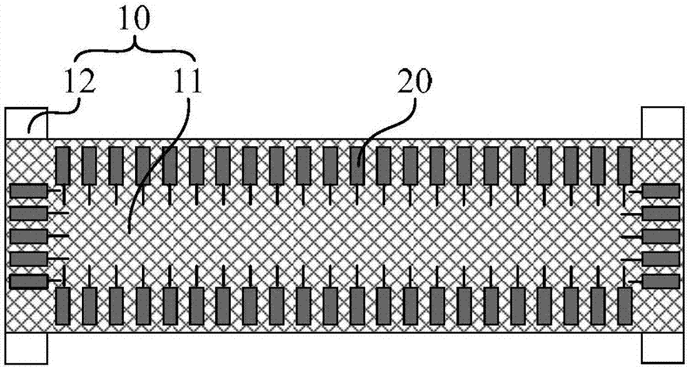
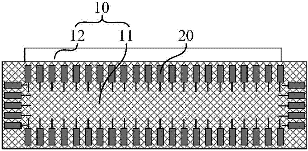
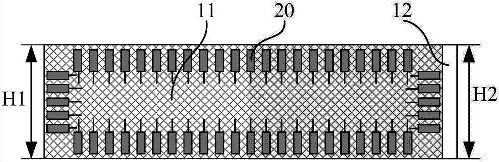
[0029] An embodiment of the present invention provides an integrated circuit chip bonding structure, such as figure 1 As shown, it includes: a substrate 10 including a functional area 11 and a dummy area 12 located around the functional area 11 on the substrate 10 . The bumps 20 of circuit components are distributed on the functional area 11 of the substrate 20 for connecting signal lines and transmitting signals.

[0030] It should be noted that, firstly, th...


PUM

PropertyMeasurementUnit
Widthaaaaaaaaaa

Abstract

The embodiment of the invention provides a binding structure of an integrated circuit chip and a display device, and relates to the technical field of display. The problem can be solved that the contact of signal lines is poor and the display effect is influenced because rolling-up and other deformation occur easily when an existing integrated circuit chip is bound with a substrate panel. The binding structure comprises a substrate and circuit-unit convex blocks, wherein the substrate is provided with a functional area and a virtual area located around the functional area; the circuit-unit convex blocks are distributed on the functional area of the substrate and used for connecting signal lines and transmitting signals. In the process of heating the binding structure of the integrated circuit chip and the display panel or binding the binding structure of the integrated circuit chip and the display panel in a pressurized mode, the virtual area arranged around the functional area can serve as a bound buffering part, rolling-up deformation defects which easily occur at the edge of the binding structure of the integrated circuit chip is limited in the virtual area, and therefore the situation is avoided that the contact of the signal lines is poor because rolling-up deformation defects occur easily to the metal convex blocks of the functional area, and the reliability of the display device is improved.

Description

technical field [0001] The invention relates to the field of display technology, in particular to an integrated circuit chip binding structure and a display device. Background technique [0002] With the continuous development of display technology, large-sized display devices, such as liquid crystal displays, LCD TVs, and flat panel displays, and small and medium-sized electronic products such as mobile phones, digital cameras, etc., are mainly developed based on lightness, thinness, shortness, and smallness. The trend is to improve the comfort of use and facilitate portability. Under this development trend, the chip bonding structure in the display module is required to be high-density and small in size, and to minimize the overall space occupation of the display device while connecting and transmitting input and output signals. [0003] In the existing integrated circuit bonding (Integrated Circuit Bonding, IC Bonding) process, the chip on glass technology (Chip on Glass...

Claims


Application Information

Patent Timeline
IPC IPC(8): G02F1/133
CPCG02F1/133
Inventor 王本莲王红丽陈立强李红王涛
Owner BOE TECH GRP CO LTD
Why Eureka
Try Eureka