Array substrate and liquid crystal display panel

A technology for liquid crystal display panels and array substrates, applied in nonlinear optics, instruments, optics, etc., can solve the problems of uncontrollable process, different exposure effects, and inability to completely block light, and achieve the effect of preventing splicing mura and avoiding color shift

Active Publication Date: 2017-10-24
TCL CHINA STAR OPTOELECTRONICS TECH CO LTD
View PDF15 Cites 15 Cited by
  • Summary
  • Abstract
  • Description
  • Claims
  • Application Information

AI Technical Summary

Problems solved by technology

However, the size (CD) stability of the exposure machine is within 3um, so for two consecutive exposures, even if the exposure parameters are set exactly the same, the obtained exposure effects will still be different, which is uncontrollable in the process of
like figure 1 As shown, in an existing large-size flat and curved shared display panel, the color filter layer 100 on the array substrate is divided into left and right regions by using the RG direct splicing technology. The R color-resist units 101' in the left area are not formed by the same exposure, and the G color-resist units 102 in the left area and the G color-resist units 102' in the right area are formed by different exposures. Therefore, the adjacent R color-resist units in the left area The width of the overlapping area between the resistance unit 101 and the G color resistance unit 102, and the relative position between the overlapping area and the corresponding data line 200 below, and the a

Method used


Image

  • Array substrate and liquid crystal display panel
  • Array substrate and liquid crystal display panel
  • Array substrate and liquid crystal display panel

Examples


Embodiment Construction

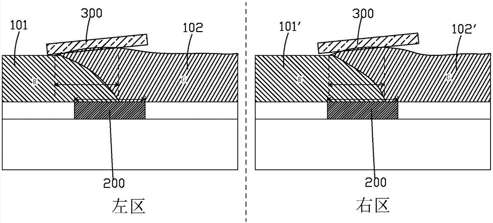
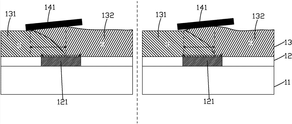
[0029] In order to further illustrate the technical means adopted by the present invention and its effects, the following describes in detail in conjunction with preferred embodiments of the present invention and accompanying drawings.

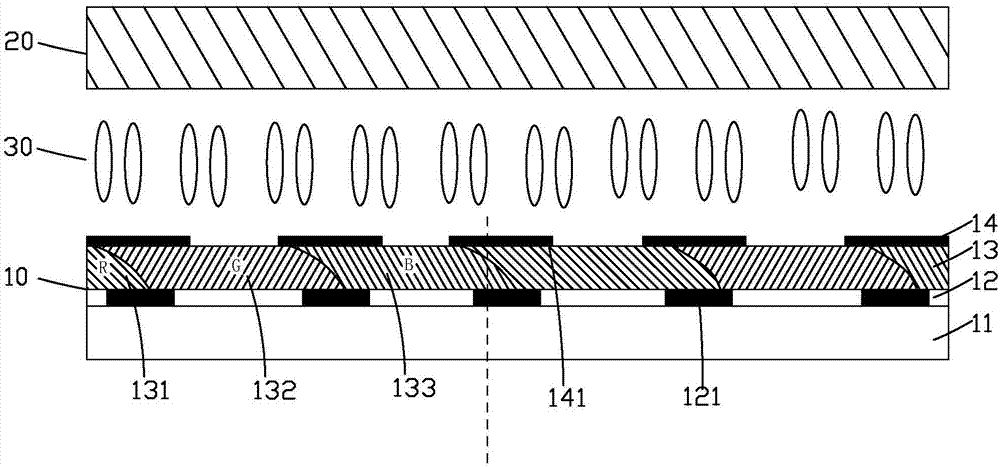
[0030] see figure 2 , the present invention provides an array substrate, comprising a base substrate 11, a TFT layer 12 disposed on the base substrate 11, a color filter layer 13 disposed on the TFT layer 12, and a color filter layer 13 disposed on the color filter A black light-shielding layer 14 on the light layer 13;

[0031] The TFT layer 12 includes a plurality of data lines 121 arranged side by side and a plurality of gate scanning lines (not shown) vertically intersecting with the data lines 121;

[0032] The color filter layer 13 includes several red color-resist units 131, several green color-resist units 132, and several blue color-resist units 133 arranged in an array, and the red color-resist units 131, green color-resist units 1...


PUM


Abstract

The invention provides an array substrate and a liquid crystal display panel. The array substrate provided by the invention comprises a substrate, a TFT layer, a colored filtering layer and a black shielding layer, wherein at least one of a red color resistance unit, a green color resistance unit and a blue color resistance unit in the colored filtering layer is prepared by fractionated exposure according to different exposure splicing areas, namely exposure by using a direct splicing technology, and the black shielding layer comprises a plurality of vertical black shielding strips correspondingly positioned above a plurality of data lines. According to the array substrate provided by the invention, the vertical black shielding strips are used for replacing DBS ITO COM lines in the prior art, difference between color resistance superposition areas on different exposure splicing areas displayed under transmission light and reflection light and the difference between the color resistance superposition areas and relative positions of the data lines below can be shielded, and thus the large-size liquid crystal display panel is prevented from generating color cast on the different exposure splicing areas of the corresponding colored filtering layer, and generation of splicing mura is avoided.

Description

technical field [0001] The invention relates to the field of liquid crystal display, in particular to an array substrate and a liquid crystal display panel. Background technique [0002] A liquid crystal display (Liquid Crystal Display, LCD) has many advantages such as a thin body, power saving, and no radiation, and has been widely used. Such as: LCD TV, mobile phone, personal digital assistant (PDA), digital camera, computer screen or laptop screen, etc. [0003] Generally, a liquid crystal display device includes a housing, a liquid crystal panel disposed in the housing, and a backlight module disposed in the housing. Among them, the structure of the liquid crystal panel is mainly composed of a thin film transistor array (Thin Film Transistor Array, TFT Array) substrate, a color filter (Color Filter, CF) substrate, that is, a color filter substrate, and a liquid crystal layer (Liquid Crystal) disposed between the two substrates. Crystal Layer), its working principle is ...

Claims


Application Information

Patent Timeline
IPC IPC(8): G02F1/1362G02F1/1335
CPCG02F1/133512G02F1/133514G02F1/136209
Inventor 黎美楠
Owner TCL CHINA STAR OPTOELECTRONICS TECH CO LTD
Why Eureka
Try Eureka