An array substrate, a liquid crystal display panel and a liquid crystal display device

A technology for an array substrate and a color filter substrate, which is applied in the field of display devices, can solve the problems of poor quality of liquid crystal display panels, color shift of liquid crystal display panels, etc., and achieves the effect of avoiding color shift and improving display quality.

Active Publication Date: 2015-11-25
XIAMEN TIANMA MICRO ELECTRONICS +1
View PDF6 Cites 11 Cited by
  • Summary
  • Abstract
  • Description
  • Claims
  • Application Information

AI Technical Summary

Problems solved by technology

In high-resolution touch screens, in order to improve the transmittance of the liquid crystal display panel, the distance between adjacent pixel electrodes in the array substrate is small. When there is an alignment deviation between the array substrate and the color filter substrate, the liquid crystal display panel is prone to color shift Phenomenon, resulting in poor quality of the LCD panel

Method used


Image

  • An array substrate, a liquid crystal display panel and a liquid crystal display device
  • An array substrate, a liquid crystal display panel and a liquid crystal display device
  • An array substrate, a liquid crystal display panel and a liquid crystal display device

Examples


no. 1 example

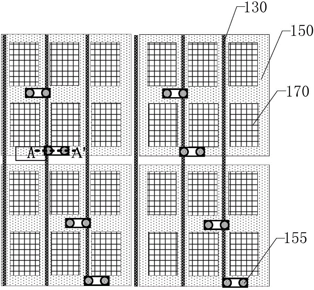
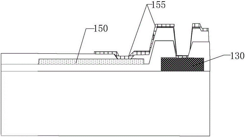
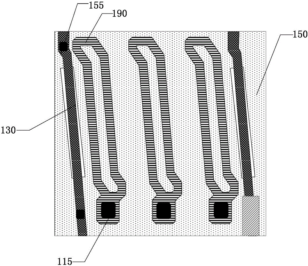
[0029] Figure 1a It is a partial top view diagram of the array substrate in the existing self-capacitance in-cell touch screen, Figure 1b for along Figure 1a Schematic cutaway of A-A'. combine Figure 1a and Figure 1b , the array substrate includes a plurality of common electrode blocks 150 and a plurality of sensing lines 130 , the common electrode blocks 150 are used for sensing user touch, and each sensing line 130 is electrically connected to a corresponding common electrode block 150 . Specifically, optionally, the sensing line 130 and the corresponding common electrode block 150 are electrically connected through the bridging structure 155, wherein the bridging structure 155 and the pixel electrode 170 are formed using the same metal layer, and the pixel electrode 170 is formed through the drain contact hole 115 is connected to the drain of the thin film transistor.

[0030] Wherein, the array substrate further includes a planarization layer 120 , a film layer wher...

no. 2 example

[0048] The second embodiment of the present invention also provides an array substrate. Figure 2a A schematic partial top view of an array substrate provided in the second embodiment of the present invention. see Figure 2a , the embodiment of the present invention and the first embodiment Figure 1e The arrangement of the auxiliary wires is the same, the difference is that each pixel electrode 170 is electrically connected to at least one auxiliary wire 180 .

[0049] The storage capacitor of the array substrate is mainly composed of the pixel electrode 170 and the common electrode block 150 . In a high-resolution touch screen, the smaller area of ​​the pixel electrode 170 leads to a lower storage capacitance, which makes the existing high-resolution liquid crystal display panels prone to display defects such as flicker and crosstalk.

[0050] Figure 2b for along Figure 2a Schematic cutaway of BB'. combine Figure 2a and Figure 2b , in this embodiment, at least on...

no. 3 example

[0060] Based on the above embodiments, the third embodiment of the present invention provides an array substrate. The array substrate includes adjacent first pixel units, second pixel units, third pixel units and fourth pixel units, wherein there are two auxiliary wires between the adjacent first pixel units and the second pixel units, each At least one pixel electrode in each pixel unit is electrically connected to one of the auxiliary wires; there are two auxiliary wires between the adjacent third pixel unit and the fourth pixel unit, and at least one pixel electrode in each pixel unit is connected to one of the auxiliary wires. The auxiliary wires are electrically connected; there is no auxiliary wire between adjacent second pixel units and third pixel units.

[0061] image 3 It is a schematic partial top view of an array substrate provided by the third embodiment of the present invention. Such as image 3 As shown, there is a first auxiliary wire 181 and a second auxil...


PUM


Abstract

The invention provides an array substrate, a liquid crystal display panel and a liquid crystal display device. The array substrate comprises: scanning lines and data lines intersecting each other to define a plurality of pixel units, each pixel unit comprising a thin film transistor and a pixel electrode connected to the thin film transistor; a plurality of common electrode blocks used for sensing the touch of users; a plurality of sensing lines each of which is electrically connected with one corresponding common electrode block; and a plurality of auxiliary conductors arranged on the same layer as the sensing lines. Each auxiliary conductor is located between two adjacent sensing lines and the auxiliary conductors are insulated from the common electrode blocks. The sensing lines and the auxiliary conductors in the array substrate together block light, so that the problems that the phenomenon of color cast occurs if contraposition bias exists between the array substrate and a colored film substrate in the liquid crystal panel with the array substrate, and the display quality of the liquid crystal display panel is improved.

Description

technical field [0001] The present invention relates to a display device, in particular to an array substrate, a liquid crystal display panel and a liquid crystal display device. Background technique [0002] Liquid crystal displays (Liquid Crystal Displays, LCDs) are widely used in various display devices such as smart phones, notebook computers, and monitors due to advantages such as good portability and low power consumption. [0003] Currently, touch screens can be classified into plug-in touch screens, surface-covered touch screens, and built-in touch screens according to the positions of touch electrodes. Among them, the plug-in touch screen directly adds touch electrodes outside the LCD. This method makes the overall thickness of the whole machine thicker and the light transmittance becomes lower. Covering the surface touch screen is to make touch electrodes outside the color film substrate of the LCD. This method reduces the thickness of the whole machine, but incre...

Claims


Application Information

Patent Timeline
Patent Type & Authority Applications(China)
IPC IPC(8): G02F1/1333G02F1/1362G06F3/041
Inventor 吴昊
Owner XIAMEN TIANMA MICRO ELECTRONICS
Why Eureka
Try Eureka