LCD (liquid crystal display) panel and manufacturing method thereof

A technology for liquid crystal display panels and manufacturing methods, applied in lighting devices, optics, light sources, etc., capable of solving problems such as color shift and affecting the display effect of liquid crystal display panels, achieving good monochromaticity, improving display effects, and avoiding color shift Effect

Inactive Publication Date: 2012-09-05
BEIJING BOE OPTOELECTRONCIS TECH CO LTD
View PDF7 Cites 12 Cited by
  • Summary
  • Abstract
  • Description
  • Claims
  • Application Information

AI Technical Summary

Problems solved by technology

[0004] Since the white light emitted by the white LED backlight is mixed with light of various wavelengths, when the white light passes through the liquid crystal layer, the optical anisotropy

Method used


Image

  • LCD (liquid crystal display) panel and manufacturing method thereof
  • LCD (liquid crystal display) panel and manufacturing method thereof
  • LCD (liquid crystal display) panel and manufacturing method thereof

Examples


Embodiment 1

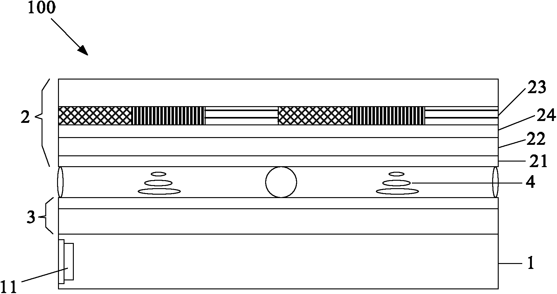
[0023] The liquid crystal display panel 100 provided by the embodiment of the present invention, such as figure 1 As shown, it includes: an LED backlight source 1, a color filter substrate 2 and a TFT array substrate 3 formed in a box, and a liquid crystal layer 4 located between the color filter substrate 2 and the TFT array substrate 3, wherein the color filter substrate 2 includes an orientation Film 21, common electrode layer 22 and color filter 23 (in figure 1 , the blue filter is represented by a vertical line filled area, the red filter is represented by a horizontal line filled area, and the green filter is represented by a grid line filled area). Further, the LED backlight 1 is a plurality of primary color LED chips 11; and on the color filter substrate 2, between the alignment film 21 and the color filter 23, a phosphor layer in which the primary color LED chips 11 form a complementary color is arranged. twenty four.

[0024] For example, if the primary color LED c...

Embodiment 2

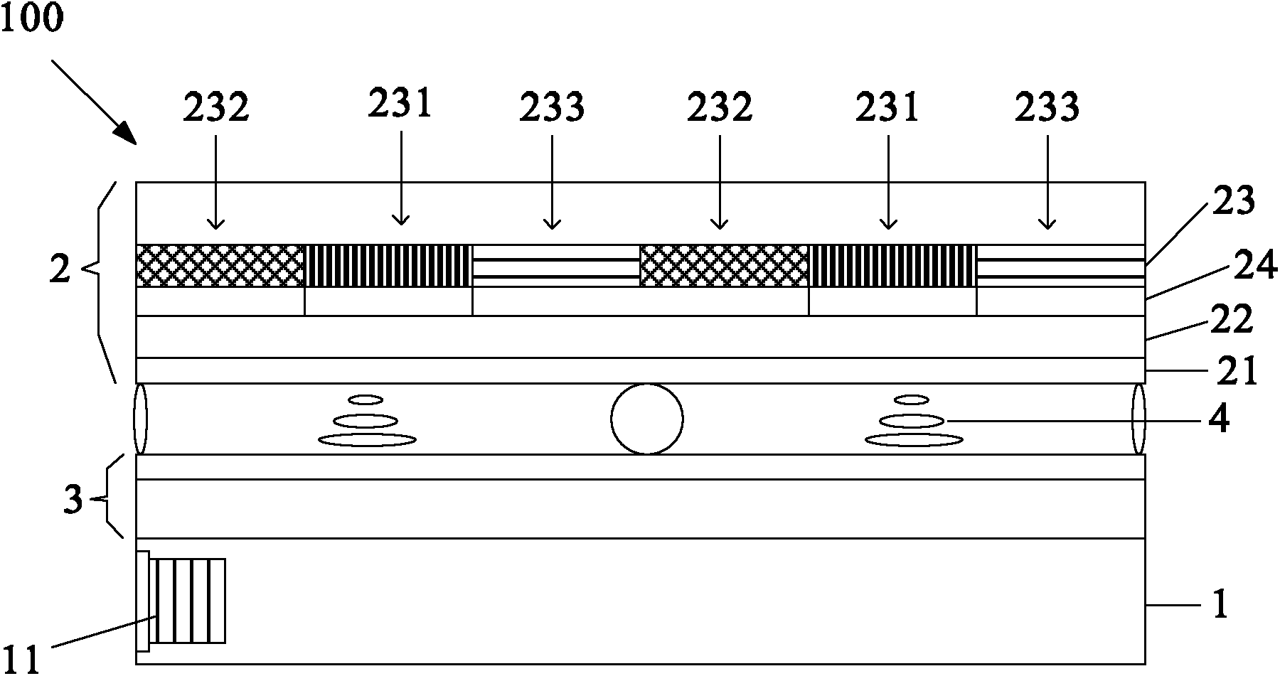
[0029] The liquid crystal display panel 100 provided by the embodiment of the present invention, such as figure 2 As shown, it includes: an LED backlight source 1, a color filter substrate 2 and a TFT array substrate 3 formed in a box, and a liquid crystal layer 4 located between the color filter substrate 2 and the TFT array substrate 3, wherein the color filter substrate 2 includes an orientation Film 21, common electrode layer 22 and color filter 23 (in figure 2 , the blue filter is represented by a vertical line filled area, the red filter is represented by a horizontal line filled area, and the green filter is represented by a grid line filled area). Further, the LED backlight 1 is a plurality of primary color LED chips 11; and on the color filter substrate 2, between the alignment film 21 and the color filter 23, a phosphor layer of the complementary color of the primary color LED chips 11 is arranged. twenty four.

[0030] In this embodiment, it is assumed that the ...

Embodiment 3

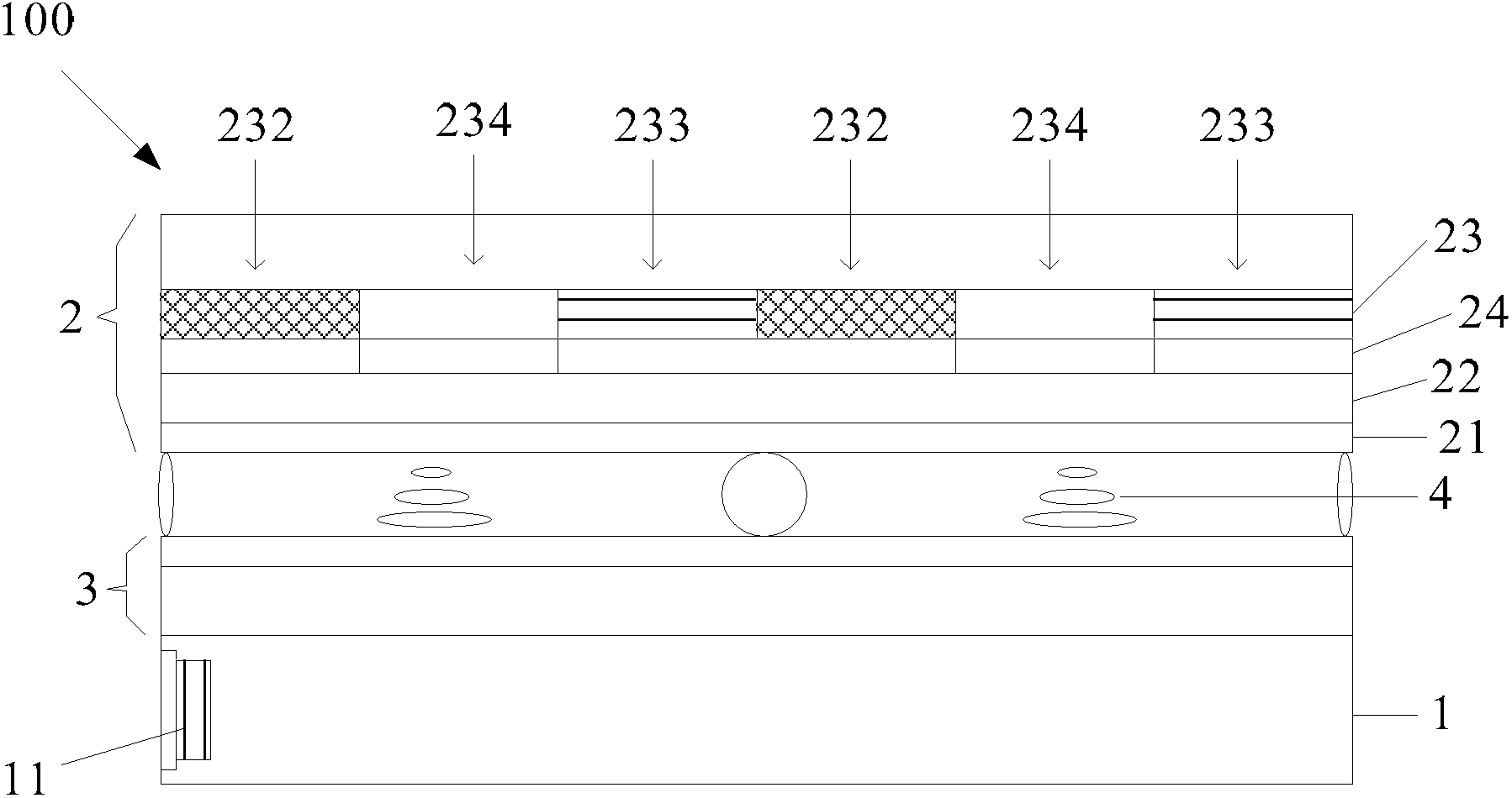
[0035] The liquid crystal display panel 100 provided by the embodiment of the present invention, such as image 3 As shown, it includes: an LED backlight source 1, a color filter substrate 2 and a TFT array substrate 3 formed in a box, and a liquid crystal layer 4 located between the color filter substrate 2 and the TFT array substrate 3, wherein the color filter substrate 2 includes an orientation Film 21, common electrode layer 22 and color filter 23 (in figure 2 , the blue filter is represented by a vertical line filled area, the red filter is represented by a horizontal line filled area, and the green filter is represented by a grid line filled area). Further, the LED backlight 1 is a plurality of primary color LED chips 11; and on the color filter substrate 2, between the alignment film 21 and the color filter 23, a phosphor layer of the complementary color of the primary color LED chips 11 is arranged. twenty four.

[0036] In this embodiment, it is assumed that the p...


PUM


Abstract

The invention provides a LCD (liquid crystal display) panel and a manufacturing method thereof, relates to the field of manufacturing of liquid crystal displays, and the LCD panel can avoid color cast of a display panel caused by different phase differences formed when visible lights with different wavelengths transmitted by a conventional white backlight pass through a liquid crystal layer. The LCD panel comprises an LED (light-emitting diode) backlight, a color film substrate molded by paired boxes, a TFT (thin film transistor) array substrate, and a liquid crystal layer positioned between the color film substrate and the TFT array substrate, wherein the color film substrate comprises an orientation film, a common electrode layer and a color filter, the LED backlight comprises a plurality of primary LED chips, and phosphor layers in complementary color with the primary LED chips are arranged on the color film substrate and between the orientation film and the color filter. The method provided by the invention is used for manufacturing the LCD panel.

Description

technical field [0001] The invention relates to the field of liquid crystal display manufacturing, in particular to a liquid crystal display panel and a manufacturing method thereof. Background technique [0002] TFT-LCD (Thin Film Transistor-Liquid Crystal Display, Thin Film Field Effect Transistor Liquid Crystal Display) uses the change of the electric field intensity set on the liquid crystal layer to change the degree of rotation of liquid crystal molecules, thereby controlling the intensity of light transmission to display images . Generally speaking, a complete liquid crystal display panel must be composed of a backlight module, a polarizer, a color filter substrate, a TFT array substrate, and a liquid crystal molecule layer filled in a box composed of these two substrates. [0003] Now, in the backlight module, the white LED backlight is gradually replacing the traditional fluorescent lamp backlight due to its low power consumption and other advantages. At present, ...

Claims


Application Information

Patent Timeline
IPC IPC(8): G02F1/13357G02F1/1335G02F1/1333F21V9/10F21Y101/02F21V9/40F21Y115/10
Inventor 林丽锋
Owner BEIJING BOE OPTOELECTRONCIS TECH CO LTD
Why Eureka
Try Eureka