Manufacturing method of crystalline silicon battery piece

A manufacturing method and technology of crystalline silicon cells, applied in the direction of final product manufacturing, sustainable manufacturing/processing, circuits, etc., can solve the problems of enterprise economic loss, appearance identification, and trouble shooting of manufacturing enterprises, so as to solve the problems of whitening after sintering, The effect of anti-PID function improvement

Active Publication Date: 2017-11-03
선테크파워컴퍼니리미티드
View PDF3 Cites 3 Cited by
  • Summary
  • Abstract
  • Description
  • Claims
  • Application Information

AI Technical Summary

Problems solved by technology

Currently O 3 Oxidation anti-PID method can greatly improve the reliability of anti-PID in the industry, but it also introduces a new problem of whitening after sintering. At the same time, because this appearance difference cannot be identified after PECVD coating, it brings great troubles to the investigation and solution process of manufacturing enterprises.
[0003] Compared with conventional stains, whitening after sintering cannot be distinguished by PECVD appearance, which brings great troubles to manufacturing companies.
At the same time, since this problem can only be found in the finished battery after printing, it can only be downgraded, which will bring economic losses to the enterprise.

Method used


Image

  • Manufacturing method of crystalline silicon battery piece
  • Manufacturing method of crystalline silicon battery piece

Examples


Embodiment Construction

[0019] In order to describe the technical content of the present invention more clearly, further description will be given below in conjunction with specific embodiments.

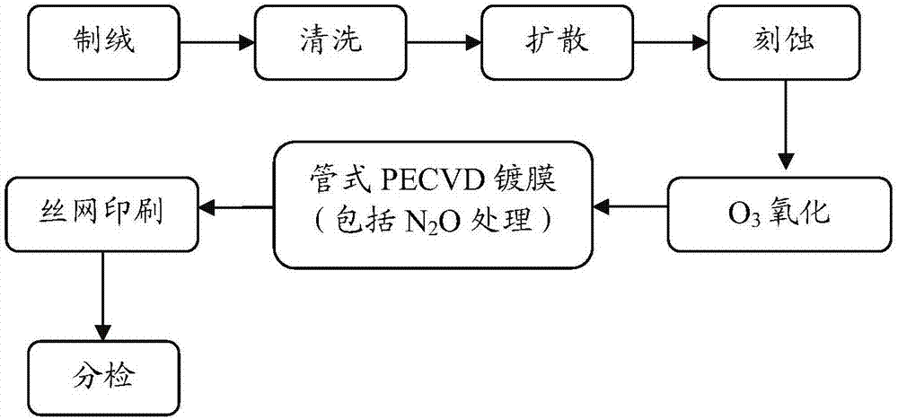
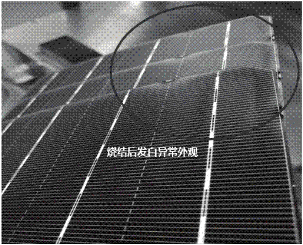
[0020] The manufacturing method of the crystalline silicon battery sheet of the present invention comprises the tubular PECVD coating step, and the described tubular PECVD coating step comprises carrying out N in the tubular PECVD. 2 O treatment and at least two silicon nitride layer coatings, said N after the first silicon nitride layer coating 2 O treatment, the crystalline silicon battery sheet has no whitening phenomenon after sintering and has anti-PID performance.

[0021] In a specific embodiment provided by the present invention, said N 2 O treatment to purge the silicon nitride layer to form N 2 Oxide layer.

[0022] In a specific embodiment provided by the present invention, said N 2 The process parameters in the O treatment include: power 5000-6500w, pressure 1600-2500mtorr, flow rate 3000-60...


PUM

PropertyMeasurementUnit
thicknessaaaaaaaaaa
thicknessaaaaaaaaaa
thicknessaaaaaaaaaa

Abstract

The invention relates to a manufacturing method of a crystalline silicon battery piece. The manufacturing method comprises a tubular PECVD film coating step, wherein the tubular PECVD film coating step comprises the steps of carrying out N2O treatment and silicon nitride silicon nitride layer film coating at least twice on tubular PECVD, and carrying out N2O treatment after the first time of silicon nitride layer film coating; and the crystalline silicon battery piece is free of whitening after sintering and is of PID resistance. By adopting the manufacturing method of the crystalline silicon battery piece in the battery, under the condition that the film thickness refractive index is unchanged, an original mono-layer SiNx film is changed into a double-layer or multi-layer SiNx film (inner-layer high refractive index SiN1 and outer-layer low refractive index SiN2), and simultaneously N2O is added after SiN2 for carrying out oxidation blowing cleaning on the surface, so that the whitening problem after sintering can be solved, and additional benefits of PID resistance promotion caused by the fact that the N2O is of oxidation capacity are also brought.

Description

technical field [0001] The present invention relates to the technical field of crystalline silicon solar cells, in particular to a manufacturing method, in particular to a manufacturing method of crystalline silicon solar cells. Background technique [0002] With the continuous improvement of the industry level, customers have higher and higher requirements on the quality of anti-PID products. From the original PECVD high refractive index anti-PID method, to N 2 O pretreatment anti-PID method, and then to the current mainstream after etching O 3 Oxidation anti-PID method (that is, the surface of the silicon wafer is covered with a layer of O 3 oxide layer). Currently O 3 Oxidation anti-PID method can greatly improve the reliability of anti-PID in the industry, but it also introduces a new problem of whitening after sintering. At the same time, because this appearance difference cannot be identified after PECVD coating, it brings great troubles to the investigation and so...

Claims


Application Information

Patent Timeline
Patent Type & Authority Applications(China)
IPC IPC(8): H01L31/18
CPCH01L31/1804Y02P70/50
Inventor 王斌何悦周东王在发任勇
Owner 선테크파워컴퍼니리미티드
Why Eureka
Try Eureka