Wafer fixing surface paste method, SMT printing steel mesh and wafer fixing device

A technology of wafer fixing and printing stencil, which is applied in printed circuit, printed circuit manufacturing, printed circuit assembly of electrical components, etc., can solve the problems of wafer cracking, product scrapping, complicated packaging process, etc., and reduce the size of bubbles Quantity, the effect of reducing voids

Pending Publication Date: 2017-11-14
UTAC DONGGUAN
View PDF5 Cites 5 Cited by
  • Summary
  • Abstract
  • Description
  • Claims
  • Application Information

AI Technical Summary

Problems solved by technology

Especially due to the complex chip packaging process, after completing the thin wafer bonding / fixing process, gold wire welding (connecting the wafer and substrate), injection molding (black glue wrapping the wafer) and other processes are required, which will affect the thin wafer. Pressure is generated especially at the void position, causing the wafer to crack, resulting in product scrapping

Method used


Image

  • Wafer fixing surface paste method, SMT printing steel mesh and wafer fixing device
  • Wafer fixing surface paste method, SMT printing steel mesh and wafer fixing device
  • Wafer fixing surface paste method, SMT printing steel mesh and wafer fixing device

Examples


Embodiment Construction

[0036] In order to describe the technical content, structural features, achieved goals and effects of the present invention in detail, the following will be described in detail in conjunction with the embodiments and accompanying drawings.

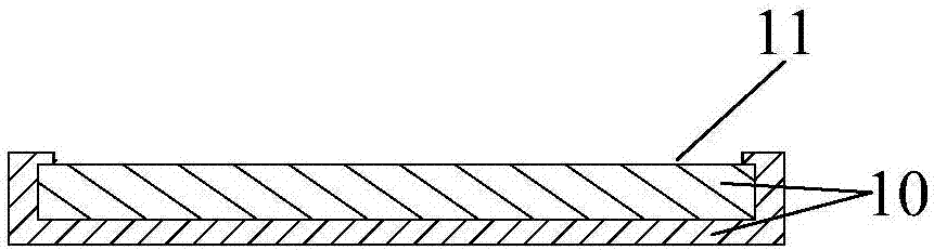
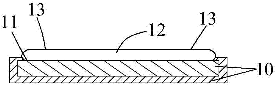
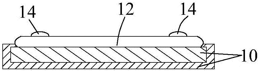
[0037] refer to Figure 1a to Figure 1e , the invention discloses a surface-attaching method for fixing a wafer, comprising the following steps: (1) referring to Figure 1a to Figure 1b , printing solder paste on the primary solder paste printing area 11 on the substrate 10 to form a primary solder paste layer 12; (2) heating and cooling the substrate 10 to volatilize the flux in the primary solder paste layer 12; (3) Reference Figure 1b with Figure 1c , printing solder paste on the secondary solder paste printing area 13 on the cooled primary solder paste layer 12 to form a secondary solder paste layer 14, the area of ​​the secondary solder paste layer 14 is smaller than the primary solder paste layer Layer 12; (4) Ref Figure 1d , t...


PUM


Abstract

The invention discloses a wafer fixing surface paste method to fix and attach a wafer on a substrate. The method comprises the steps that solder paste is printed in a primary solder paste printing area on the substrate to form a primary solder paste layer; the substrate is heated and cooled to volatilize a flux in the primary solder paste layer; solder paste is printed in a secondary solder paste printing area on the cooled primary solder paste layer to form a secondary solder paste layer, wherein the area of the secondary solder paste layer is smaller than the area of the primary solder paste layer; the wafer is attached on the substrate through the secondary solder paste layer; and reflow soldering is carried out on the substrate on which the wafer is attached to fix and attach the wafer on the substrate. Compared with the prior art, the method provided by the invention has the advantages that a part of the solder paste which is not attached is heated to volatilize the flux, which effectively reduces the size and number of the bubbles generated by heating after sticking; and the method can be used for fixing and attaching a thin wafer. The invention further discloses an SMT printing steel mesh and an SMT wafer fixing device.

Description

technical field [0001] The invention relates to an SMT process, in particular to a device and a method for pasting and fixing a wafer on a substrate in the SMT process. Background technique [0002] The existing method of fixing the wafer with solder paste (Solder Die Attach) adopts the printing method of solder paste. After the solder paste is printed from the stencil to the substrate, the wafer / component is then pasted, and the solder paste is soldered through the reflow furnace. Wafers / components etc. are fixed on the substrate. [0003] However, due to the flux (rosin) contained in the solder paste material, since the volatilization of the flux is hindered after the wafer is attached, it will become air bubbles and remain at the bottom of the wafer during subsequent reflow soldering, forming solder voids. For thicker wafers, solder voids will not cause serious problems, but with the development of wafer technology, the thickness of wafers becomes thinner, and the risk o...

Claims


Application Information

Patent Timeline
Patent Type & Authority Applications(China)
IPC IPC(8): H05K3/34
CPCH05K3/341H05K2203/04
Inventor 林永强艾米塔陈勃宏甘景文麦子永陈钦生王鹏罗尔·A·罗夫莱斯郑瑞育吴进瑜商峰旗
Owner UTAC DONGGUAN
Why Eureka
Try Eureka