Display panel, display apparatus and manufacturing method of display panel

A technology for a display panel and a manufacturing method, which is applied to the manufacturing of semiconductor/solid-state devices, organic semiconductor devices, electrical components, etc., can solve the problems of unsatisfactory display effect, uneven voltage distribution, poor uniformity of display images, etc., and achieves improved image uniformity. The effect of improving the display effect and improving the transmittance

Inactive Publication Date: 2017-11-17
SHANGHAI TIANMA AM OLED
View PDF16 Cites 15 Cited by
  • Summary
  • Abstract
  • Description
  • Claims
  • Application Information

AI Technical Summary

Problems solved by technology

However, according to the square resistance R s =Resistivity ρ / thickness t, the smaller the value of thickness t, the square resistance R s The larger the value, the greater the voltage drop in the common cathode layer on the entire surface, and the uneven voltage distribution, which will lead to poor uniformity of the display screen and unsatisfactory display effect. For high-resolution products, the impact is more obvious

Method used


Image

  • Display panel, display apparatus and manufacturing method of display panel
  • Display panel, display apparatus and manufacturing method of display panel
  • Display panel, display apparatus and manufacturing method of display panel

Examples


Embodiment Construction

[0024] In order to reduce the in-plane voltage drop of the entire common cathode layer, increase the transmittance of the entire common cathode layer, and further improve the display effect, the embodiments of the present invention provide a display panel, a display device, and a method for manufacturing the display panel. In order to make the purpose, technical solution and advantages of the present invention clearer, the following examples are given to further describe the present invention in detail.

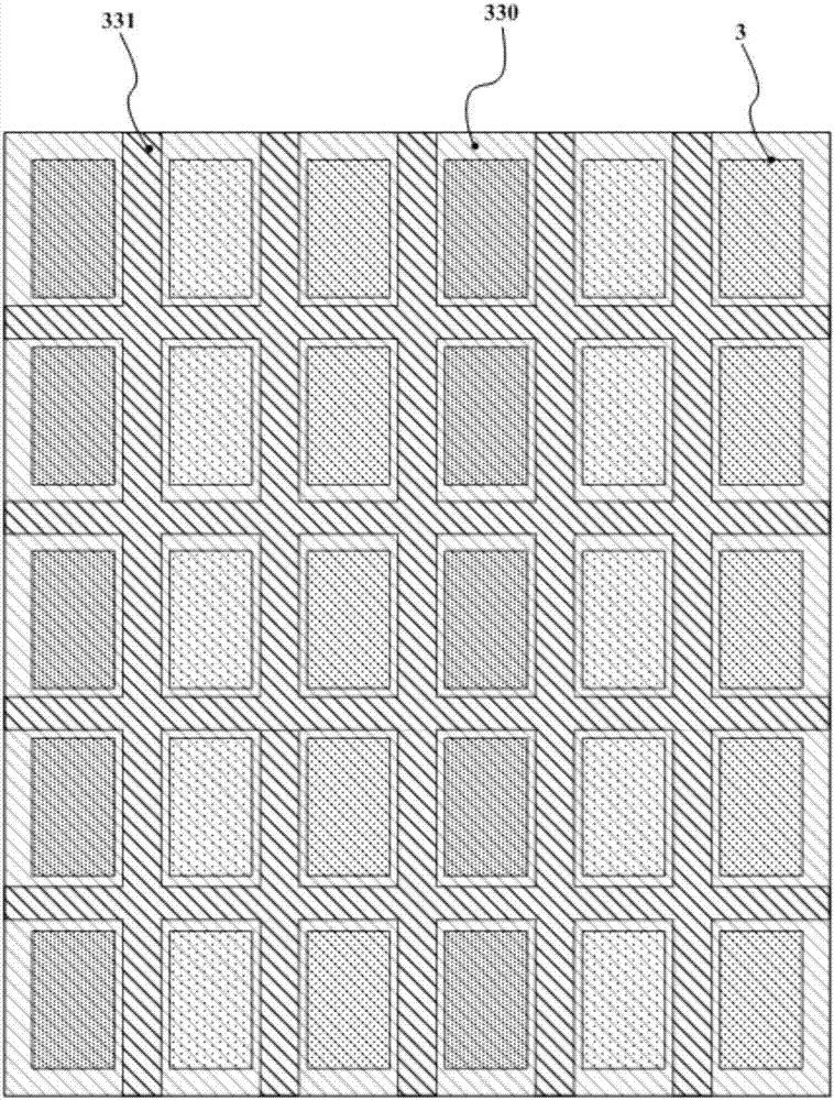
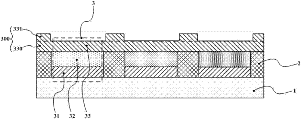
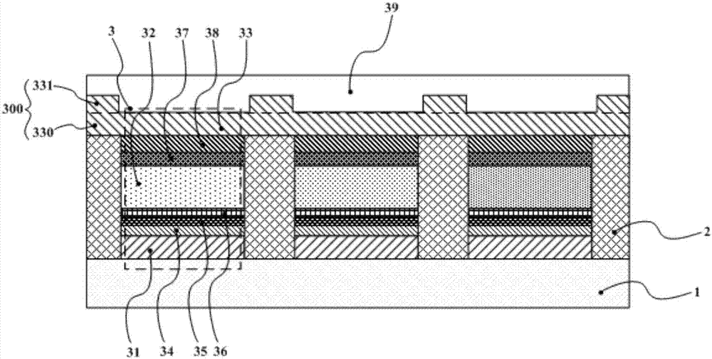
[0025] Such as figure 1 with figure 2 As shown, the display panel provided by this embodiment of the present invention includes a base substrate 1, a pixel definition layer 2 and a plurality of light-emitting devices 3 disposed on one side of the base substrate 1, and the pixel definition layer 2 defines a plurality of opening units , the aforementioned plurality of light-emitting devices 3 are set corresponding to the aforementioned plurality of opening units, wherein:

...


PUM


Abstract

The invention discloses a display panel, a display apparatus and a manufacturing method of the display panel, aiming at reducing the in-plane voltage drop of an entire surface shared cathode layer, increasing the transmittance of the entire surface shared cathode layer, and further increasing display effects. The display panel includes a liner substrate, and a pixel defining layer and a plurality of light-emitting devices which are disposed on one side of the substrate. The pixel defining layer defines a plurality of opening units. The plurality of light-emitting devices are disposed corresponding to the plurality of opening units. Each light-emitting device includes an anode, a light-emitting layer and a cathode which are successively arranged distant from the substrate. The cathodes of the light-emitting devices are connected into the entire surface shared cathode layer which includes a body layer and a protruding mechanism which is disposed on one side of the body layer distant from the substrate and is opposite to the position of the pixel defining layer.

Description

technical field [0001] The present invention relates to the field of display technology, in particular to a display panel, a display device and a manufacturing method of the display panel. Background technique [0002] OLED (organic light-emitting diode, organic light-emitting diode) can be divided into PM (Passive Matrix, passive matrix drive) OLED and AM (Active Matrix, active matrix drive) OLED according to different driving methods. Among them, AMOLED is widely used in flat panel display devices of various sizes because an independent TFT (Thin Film Transistor, thin film transistor) is used to control each pixel unit, and each pixel unit can continuously and independently emit light. [0003] AMOLED can be divided into top-emission type and bottom-emission type according to different light emitting methods. Because the pixel aperture ratio of the top-emission type is relatively large, the top-emission type structure is mostly used in the industry at present. There is an...

Claims


Application Information

Patent Timeline
Patent Type & Authority Applications(China)
IPC IPC(8): H01L51/52H01L51/56H01L27/32
CPCH10K59/12H10K50/822H10K2102/3026H10K71/00
Inventor 辛宇
Owner SHANGHAI TIANMA AM OLED
Why Eureka
Try Eureka