Array substrate, preparation method of array substrate, and display panel

An array substrate and substrate substrate technology, which is applied in static indicators, semiconductor/solid-state device manufacturing, instruments, etc., can solve the problems of unobstructed, unstable thin-film transistors, etc., and achieve the effect of strong practicability

Active Publication Date: 2017-11-21
BOE TECH GRP CO LTD +1
View PDF6 Cites 17 Cited by
  • Summary
  • Abstract
  • Description
  • Claims
  • Application Information

AI Technical Summary

Problems solved by technology

[0003] However, in order to protect the stability of the channel layer in large-size OLEDs, a layer of metal pattern will be formed under the top-gate thin-film transistor to avoid the interference of external light on its characteristics, but this will produce a double thin-film transistor effect.
Moreover, because there is a buffer layer between the metal pattern and the channel layer, and the large-size OLED metal wiring is very dense, it cannot block the light reflected by other metal regions, resulting in instability of the thin film transistor.

Method used


Image

  • Array substrate, preparation method of array substrate, and display panel
  • Array substrate, preparation method of array substrate, and display panel
  • Array substrate, preparation method of array substrate, and display panel

Examples


Embodiment Construction

[0052] The following will clearly and completely describe the technical solutions in the embodiments of the present invention with reference to the accompanying drawings in the embodiments of the present invention. Obviously, the described embodiments are only some, not all, embodiments of the present invention. Based on the embodiments of the present invention, all other embodiments obtained by persons of ordinary skill in the art without making creative efforts belong to the protection scope of the present invention.

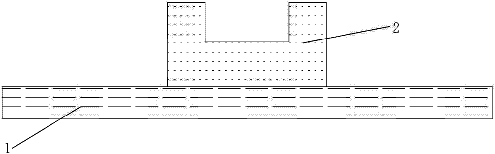
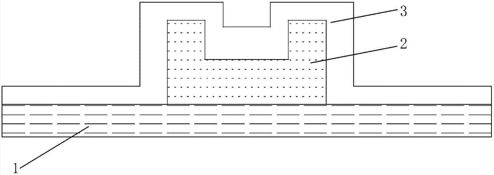
[0053] Please refer to Figure 2i , the present invention provides an array substrate, including a base substrate 1 and a plurality of thin film transistor switches arrayed on the base substrate 1, and each thin film transistor switch includes:

[0054]A light-shielding block formed on the base substrate 1 and formed of a non-metallic material, the light-shielding block is formed with a first groove whose opening direction is away from the base substrate 1;

...


PUM


Abstract

The invention relates to the technical field of display, and discloses an array substrate, a preparation method of the array substrate, and a display panel. The array substrate comprises an underlayer substrate and a plurality of thin film transistor (TFT) switches, wherein each TFT switch comprises a light shielding block formed on the underlayer substrate, a buffer layer formed on one side, deviated from the underlayer substrate, of each light shielding block, a channel layer formed in a second groove, and a grid insulating layer, a grid electrode, an interlayer insulating layer, a source-drain electrode and a passivation layer formed on one side, deviated from the underlayer substrate, of each channel layer; first grooves with opening directions deviated from the underlayer substrate are formed in the light shielding blocks; and the second grooves are formed in the buffer layers corresponding to the first grooves. According to the array substrate, the light shielding blocks are prepared by non-metal materials, so that a double TFT effect can be avoided; and bulges on the two sides of the first grooves are utilized to shield light without a TFT switch region, so that the stability of the TFT switches can be improved.

Description

technical field [0001] The invention relates to the field of display technology, in particular to an array substrate, a preparation method thereof, and a display panel. Background technique [0002] Recently, Organic Light-Emitting Diode (OLED) has gradually become the mainstream of display panels due to its advantages of high contrast ratio and self-luminescence, and is favored by the public. [0003] However, in order to protect the stability of the channel layer in large-size OLEDs, a layer of metal pattern is formed under the top-gate TFT to avoid external light from interfering with its characteristics, but this will result in a double TFT effect. Moreover, since there is a buffer layer between the metal pattern and the channel layer, and the large-size OLED metal wiring is very dense, it cannot block the light reflected by other metal regions, resulting in instability of the thin film transistor. Contents of the invention [0004] The invention provides an array sub...

Claims


Application Information

Patent Timeline
Patent Type & Authority Applications(China)
IPC IPC(8): H01L27/12H01L27/32H01L29/786H01L21/77
CPCH01L27/1225H01L27/127H01L27/1296H01L29/78633H10K59/12H01L27/1218H01L29/7869H01L29/78696G09G3/3225H01L27/1259H01L29/41733
Inventor 刘军李伟周斌苏同上方金钢张扬
Owner BOE TECH GRP CO LTD
Why Eureka
Try Eureka