OLED package structure and manufacture method thereof and display device

A technology of packaging structure and film layer, which is applied in semiconductor/solid-state device manufacturing, semiconductor devices, electrical components, etc., can solve the problems of poor packaging effect of OLED packaging structure, achieve poor packaging effect, improve packaging effect, and avoid misalignment Effect

Inactive Publication Date: 2017-11-24
BOE TECH GRP CO LTD +1
View PDF4 Cites 32 Cited by
  • Summary
  • Abstract
  • Description
  • Claims
  • Application Information

AI Technical Summary

Problems solved by technology

[0006] In order to solve the problem of poor encapsulation effect of OLED encapsulation structure, the present invention provides an OLED encapsulation structure and its manufacturing method and display device

Method used


Image

  • OLED package structure and manufacture method thereof and display device
  • OLED package structure and manufacture method thereof and display device
  • OLED package structure and manufacture method thereof and display device

Examples


Embodiment Construction

[0058] In order to make the purpose, technical solutions and advantages of the present invention clearer, the present invention will be further described in detail below in conjunction with the accompanying drawings. Obviously, the described embodiments are only some of the embodiments of the present invention, rather than all of them. Based on the embodiments of the present invention, all other embodiments obtained by persons of ordinary skill in the art without making creative efforts belong to the protection scope of the present invention.

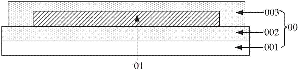
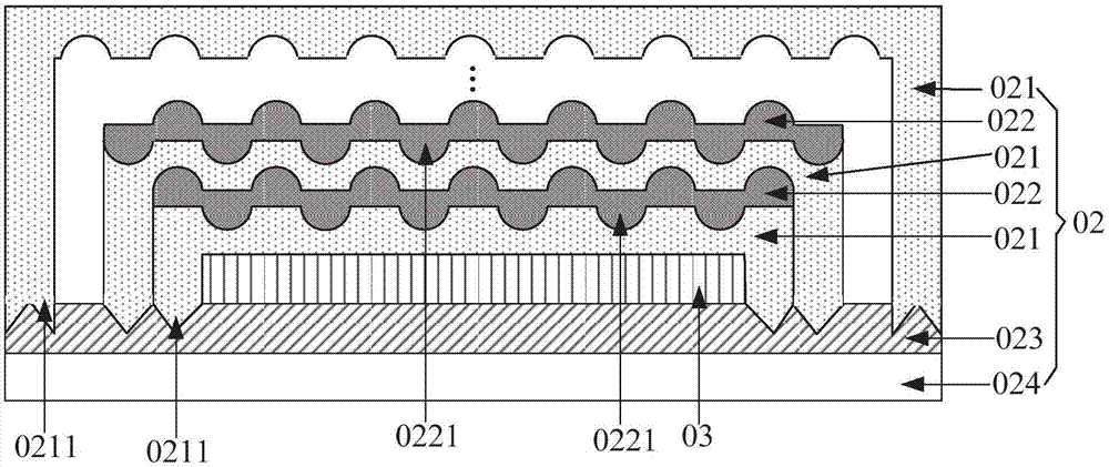
[0059] OLED devices have the advantages of thinness, low power consumption, high contrast, high color gamut, and flexible display, and are widely used in electronic products. Flexible OLED devices are the main direction of research and development in the field of display technology. As we all know, the electrode layer and organic light-emitting layer in OLED devices are very sensitive to water vapor, oxygen and other components in the ai...


PUM


Abstract

The invention discloses an OLED package structure and a manufacture method thereof and a display device, and belongs to the field of display device package. The OLED package structure comprises a plurality of film layers covering an OLED device. The plurality of film layers comprise alternately-stacked inorganic layers and organic layers; and any two mutually-contacted film layers of the plurality of film layers are in clamp connection. The OLED package structure and the manufacture method thereof and the display device solve the problem of poor package effect of the OLED package structure; and the package effect of the OLED package structure is improved. The OLED package structure and the manufacture method thereof are used for package of the OLED device.

Description

technical field [0001] The invention relates to the field of display device packaging, in particular to an OLED packaging structure, a manufacturing method thereof, and a display device. Background technique [0002] Organic Light-Emitting Diode (English: Organic Light-Emitting Diode; abbreviation: OLED) devices have the advantages of thinness, low power consumption, high contrast, high color gamut, and flexible display, and are widely used in the display industry. However, water vapor, oxygen and other components in the air usually erode OLED devices, seriously affecting the performance of OLED devices and limiting the service life of OLED devices. Therefore, it is usually necessary to use OLED packaging structures to package OLED devices to make OLED devices It is isolated from water vapor, oxygen and other components in the air, thereby reducing the influence of water vapor and oxygen in the air on the performance of OLED devices, and prolonging the service life of OLED d...

Claims


Application Information

Patent Timeline
Patent Type & Authority Applications(China)
IPC IPC(8): H01L51/52
CPCH10K50/8445H10K50/841
Inventor 张国林程久阳邹佳洪肖文豪牟良丰李俊良
Owner BOE TECH GRP CO LTD
Why Eureka
Try Eureka