Pixel driving circuit, driving method thereof, array substrate and display device

A pixel drive circuit and drive switch technology, applied to static indicators, instruments, etc., can solve the problem of uneven luminance and achieve the effect of reducing the number and control complexity

Pending Publication Date: 2017-12-15
BOE TECH GRP CO LTD
View PDF6 Cites 6 Cited by
  • Summary
  • Abstract
  • Description
  • Claims
  • Application Information

AI Technical Summary

Problems solved by technology

[0009] In order to solve the problem that the luminous current of the OLED is affected by the threshold voltage of the drive transistor and the voltage drop of the backplane power supply to produce

Method used


Image

  • Pixel driving circuit, driving method thereof, array substrate and display device
  • Pixel driving circuit, driving method thereof, array substrate and display device
  • Pixel driving circuit, driving method thereof, array substrate and display device

Examples


Embodiment 1

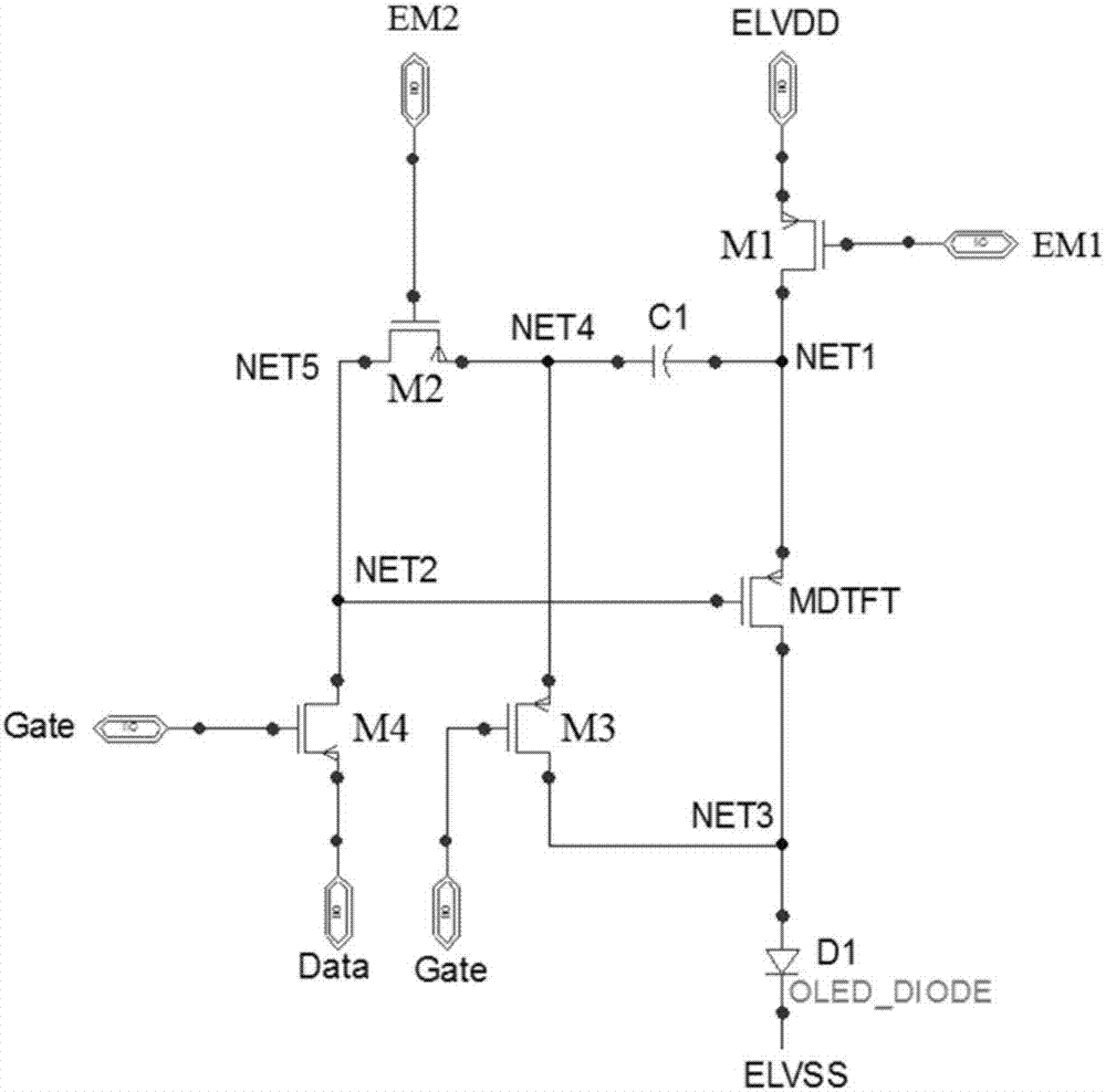
[0055] Such as figure 2 As shown, an OLED pixel driving circuit includes a driving transistor MDTFT, first to fourth transistors M1-M4 and a storage capacitor C1. The specific circuit connection relationship is as follows:

[0056] The gate of the first transistor M1 receives the first driving switch signal EM1 , the source receives the first power signal ELVDD, and the drain is connected to the source of the driving transistor MDTFT and the first terminal of the storage capacitor C1 . The first transistor M1 is turned on in response to the first driving switch signal EM1 to transmit the first power signal ELVDD to the source of the driving transistor MDTFT.

[0057] The gate of the second transistor M2 receives the second driving switch signal EM2 , the source is connected to the second end of the storage capacitor C1 , and the drain is connected to the gate of the driving transistor MDTFT. The second transistor M2 is turned on in response to the second driving switch sign...

Embodiment 2

[0092] Such as Figure 7 As shown, an OLED pixel driving circuit includes a driving transistor MDTFT, first to fifth transistors M1-M5 and a storage capacitor C1. The specific circuit connection relationship is as follows:

[0093] The gate of the first transistor M1 receives the first driving switch signal EM1 , the source receives the first power signal ELVDD, and the drain is connected to the source of the driving transistor MDTFT and the first terminal of the storage capacitor C1 . The first transistor M1 is turned on in response to the first driving switch signal EM1 to transmit the first power signal ELVDD to the source of the driving transistor MDTFT.

[0094] The gate of the second transistor M2 receives the first driving switch signal EM1 , the source is connected to the second end of the storage capacitor C1 , and the drain is connected to the source of the fifth transistor M5 . The gate of the fifth transistor M5 receives the second driving switch signal EM2 , and...

Embodiment 3

[0117] This embodiment provides an array substrate, including the pixel driving circuit described in Embodiment 1 or 2.


PUM


Abstract

The invention discloses a pixel driving circuit. The pixel driving circuit comprises a driving transistor, a first switching element, a second switching element, a third switching element, a fourth switching element and a storage capacitor. Different control signals control the on-off states of the switching elements so as to achieve the compensation function of the pixel driving circuit, and the light emitting current of an OLED is only related to a threshold voltage and data signals of the OLED and is irrelevant to a threshold voltage of the driving transistor and the voltage drop of a back plate power supply, so that the problem that the light emitting brightness is uneven due to the deviation of the threshold voltage of the driving transistor and the voltage drop of the back plate power supply is solved. The invention further discloses a driving method, an array substrate and a display device.

Description

technical field [0001] The invention relates to the technical field of organic light emitting diode display. More specifically, it relates to an OLED pixel driving circuit, a driving method thereof, an array substrate and a display device. Background technique [0002] Organic light emitting diode (Organic Light Emitting Diode, OLED) display technology refers to the technology in which organic light emitting materials are driven by current to cause light emission through carrier injection and recombination. The principle of OLED light emission is to use ITO electrodes and metal electrodes as the first pole and the second pole of the device respectively. Under a certain current drive, electrons and holes are respectively injected from the second pole and the first pole into the electron and hole transport layer. , electrons and holes migrate to the light-emitting layer through the electron and hole transport layers respectively, and recombine in the organic substance with li...

Claims


Application Information

Patent Timeline
IPC IPC(8): G09G3/3233G09G3/3291
CPCG09G3/3233G09G3/3291G09G2320/0233G09G2300/0819G09G2300/0842G09G2300/0861G09G2320/043G09G2320/045G09G2300/0809G09G2300/0426G09G2320/0257G09G2300/043
Inventor 高雪岭
Owner BOE TECH GRP CO LTD
Why Eureka
Try Eureka