A Planar Inductive Magnetic Sensor
A magnetic sensor and planar inductance technology, applied in the field of sensors, can solve the problem of not being able to be used as a low frequency, and achieve the effect of increasing the effect of self-inductance and mutual inductance
- Summary
- Abstract
- Description
- Claims
- Application Information
AI Technical Summary
Problems solved by technology
Method used
Image
Examples
Embodiment 1
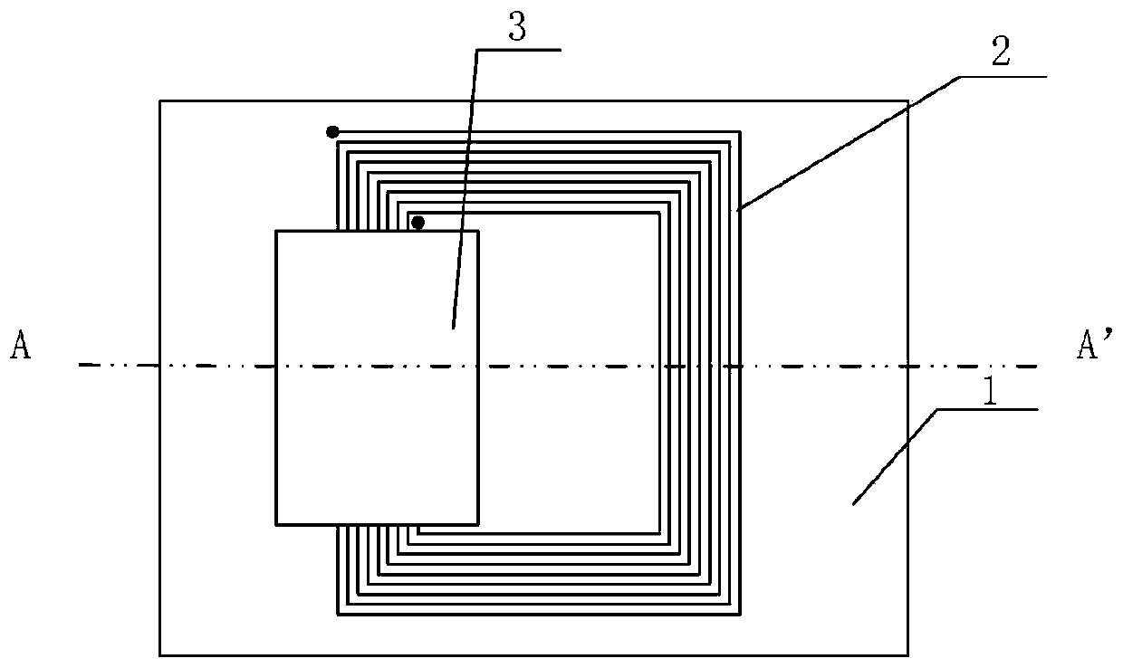
[0034] Using silicon dioxide as a substrate, a rectangular planar coil is made on it by sputtering or electroplating, and a layer of silicon dioxide film is coated on one arm of the rectangular coil, and then sputtering or electroplating is applied on the silicon dioxide film. The method makes a layer of FeNi alloy thin film layer such as Figure 1-2 as shown, Figure 1-2 They are a top view and a cross-sectional view of a planar inductive magnetic sensor of Embodiment 1, respectively.
Embodiment 2
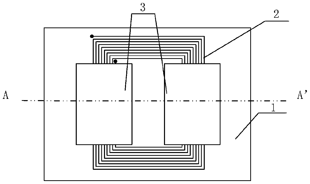
[0036] Using silicon dioxide as the substrate, a rectangular planar coil is made on it by sputtering or electroplating, and a layer of silicon dioxide film is coated on the two parallel arms of the rectangular coil, respectively. A layer of FeNi alloy film layer is made by sputtering or electroplating in the coil wire area. The alloy film layer covering the two arms of the coil is not connected, and the minimum distance is greater than the thickness of the film layer, such as Figure 3-4 as shown, Figure 3-4 They are a top view and a cross-sectional view of a planar inductive magnetic sensor according to Embodiment 2, respectively.
Embodiment 3
[0038]Using silicon dioxide as a substrate, a FeNi alloy thin film layer is made on it by sputtering or electroplating. The alloy thin film layer can be one region or multiple disconnected regions, and the minimum distance between regions is greater than that of the film. layer thickness, make a silicon dioxide film layer on the alloy film layer, make a rectangular planar coil on a substrate with an alloy film layer and a silicon dioxide insulating layer, and place an arm of the rectangular coil on an area of the alloy film layer to ensure The current direction of the coil wires in this area is the same, and the silicon dioxide film layer is covered above the coil part with the alloy layer, and then the FeNi alloy film layer is made by sputtering or electroplating, and the alloy layer covered on the pad and the liner The alloy layer at the corresponding position on the upper part is connected, such as Figure 5 as shown, Figure 5 It is a cross-sectional view of a planar in...
PUM
 Abstract
Description
Claims
Application Information


