Array substrate, display panel and display device

A technology for array substrates and display areas, which is applied in nonlinear optics, instruments, optics, etc., can solve the problems of incompatibility of array substrates, and achieve the effect of avoiding changing masks and overcoming incompatibility

Inactive Publication Date: 2018-01-05
BOE TECH GRP CO LTD +1
View PDF26 Cites 6 Cited by
  • Summary
  • Abstract
  • Description
  • Claims
  • Application Information

AI Technical Summary

Problems solved by technology

[0006] The technical problem to be solved by this application is to provide an array substrate, a display panel and a display device, which can effectively overcome the problem of incompatibility between the array substrates of existing common liquid crystal products and the array substrates of embedded touch products

Method used


Image

  • Array substrate, display panel and display device
  • Array substrate, display panel and display device

Examples


Embodiment 1

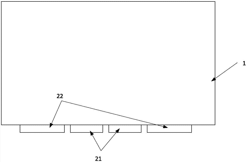
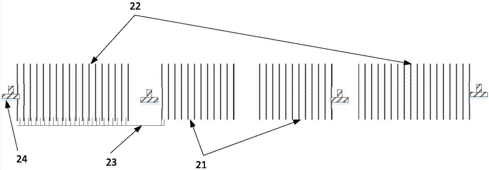
[0040] combine figure 1 , figure 2 As shown, Embodiment 1 of the present invention provides an array substrate, including a display area 1 and a frame area 2 located on the periphery of the display area 1; The bonding area 21 and two second bonding areas 22 for connecting the COF of the second specification, and the second bonding area 22 are provided with connecting electrodes 23 for connecting the first bonding area 21 .

[0041] In the specific operation, the input of the display signal required for the operation of ordinary liquid crystal products can be realized through the setting of the above-mentioned first binding area 21; the touch control of embedded touch products can be realized through the setting of the above-mentioned second binding area 22 signal input, and to realize the input of the common voltage signal of common liquid crystal products; when the product requires a touch function, the first binding area 21 is bound to the chip-on-chip film of the first sp...

Embodiment 2

[0051] Embodiment 2 of the present invention provides a display panel, including the array substrate described in Embodiment 1.

Embodiment 3

[0053] Embodiment 2 of the present invention provides a display device, including the display panel described in Embodiment 2.


PUM


Abstract

The invention discloses an array substrate, a display panel and a display device. The array substrate comprises a display area and a frame area on the periphery of the display area. Two first bindingareas for being connected with a first scale chip on film and two second binding areas for being connected with a second scale chip on film are arranged on the frame area. The second binding areas areprovided with connecting electrodes for being connected with the first binding areas. The display panel comprises the array substrate. The display device comprises the display panel. The invention can be applied to the technical field of display.

Description

technical field [0001] The present application relates to the field of display technology, in particular to an array substrate, a display panel and a display device. Background technique [0002] The in-cell touch panel (Incell Touchpanel) is different from the integrated circuit (IC) design of the ordinary liquid crystal display (Liquid Crystal Display, LCD). The pin of the touch (Touch) signal transmission line; at present, the integrated circuit design of the chip-on-flex (Chip On Flex or Chip On Film, COF) of the embedded touch product is not compatible with the ordinary liquid crystal display. [0003] For example, a 14.0 Full High Definition (FHD) high aperture ratio Advanced Super Dimensional Switching (High Aperture Advanced Super Dimensional Switching, HADS) dual gate (Dual Gate) product requires a 2880 A connecting line (Channel). Each COF with a specification of 48mm is provided with 960 connecting lines, and three COFs with a specification of 48mm are required ...

Claims


Application Information

Patent Timeline
Patent Type & Authority Applications(China)
IPC IPC(8): G02F1/1345
Inventor 李少茹汪锐
Owner BOE TECH GRP CO LTD
Why Eureka
Try Eureka