Chip testing and sealing device and technology thereof

A technology of chip testing and testing equipment, which is applied in the fields of electronic circuit testing, electrical components, semiconductor/solid-state device manufacturing, etc. It can solve the problems of poorly sealed cover tape, cover tape disengagement, maximum and minimum Gauss amount, etc., to achieve The effect of external disturbance reduction

Active Publication Date: 2018-01-19
CHANGJIANG ELECTRONICS TECH CHUZHOU
View PDF23 Cites 2 Cited by
  • Summary
  • Abstract
  • Description
  • Claims
  • Application Information

AI Technical Summary

Problems solved by technology

[0011] In the process of chip testing and packaging in the prior art, the magnetic field of the Hall coil in the test area is not stable enough, the difference between the maximum and minimum Gauss values ​​measured is large, and the position of the chip on the suction nozzle is not aligned with the POCKET entering the carrier tape. Chips are prone to warping feet, cover tape detachment and wire drawing caused by cover tape offset, and cover tape and carrier tape due to poor sealing during the sealing process, resulting in cover tape disengagement and cover tape whitening. The present invention provides a Chip testing and sealing device and its process

Method used


Image

  • Chip testing and sealing device and technology thereof
  • Chip testing and sealing device and technology thereof
  • Chip testing and sealing device and technology thereof

Examples


Embodiment 1

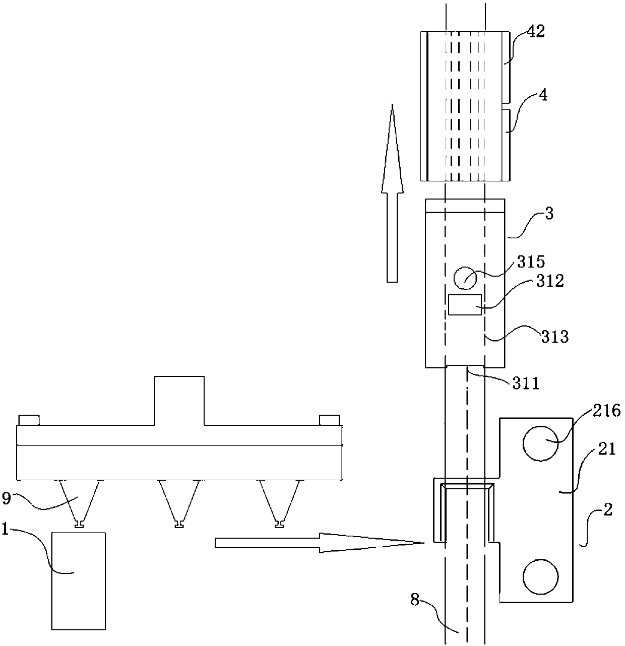
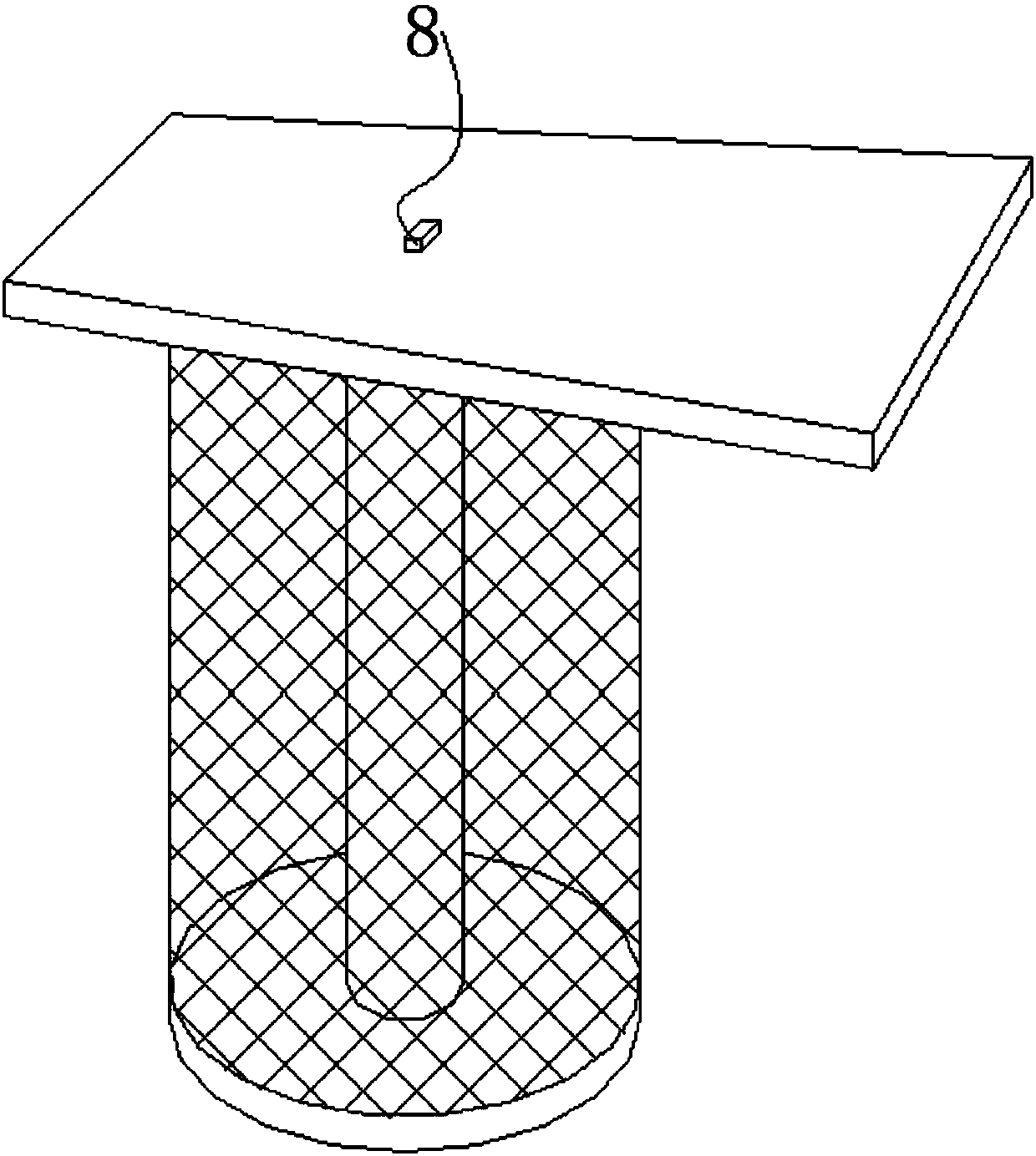
[0093] The chip testing and sealing device of the present embodiment, such as figure 1 As shown, it includes a suction nozzle 9, a test device 1, and an anti-snap into the bag mechanism 2, an anti-cover tape offset mechanism 3, and a sealing knife mechanism 4 arranged in a process sequence above the carrier tape 7. The suction nozzle 9 will test The chip 8 after the device 1 test is transferred to the anti-snap pin into the bag mechanism 2, wherein: as Figure 28 As shown, the test device 1 includes a Hall coil 11, a collar 12, a test base 13, a Hall test piece and a Hall movable clamp 16; the Hall coil includes an I-shaped support 112 and is wrapped in the middle of the I-shaped support 112. Parts of the enameled wire coil 111, such as Figure 36 , 37, 38, one end of the I-shaped bracket 112 is a ring platform 1121, and the center of the ring platform 1121 is a circular groove 1124; the center of the circular groove 1124 is a circular through hole 1123. The chip 8 can be ...

Embodiment 2

[0095] The chip testing and sealing device of present embodiment, basic structure is the same as embodiment 1, difference and improvement are: the depth of circular groove 1124 is not less than the sum of the thickness of test base 13, test piece and chip 8, with It is ensured that the chip 8 does not protrude from the circular groove 1124, thereby ensuring the stability of the test magnetic field. On the ring platform 1121 of the I-shaped bracket 112, two left and right symmetrical slots 1122 are opened outward from the circular groove 1124, providing passages for the chip 8 to enter and exit. The shape and size of the bottom of the braiding window 22 are consistent with the opening of the bag of the carrier tape 7, which is 3.3×3.2mm, forming a straight drop microchannel of the chip to avoid secondary offset when the chip is inserted; Mechanism and directional track mechanism cooperate to realize, and elastic mechanism realizes the purpose of buffering, and directional track...

Embodiment 3

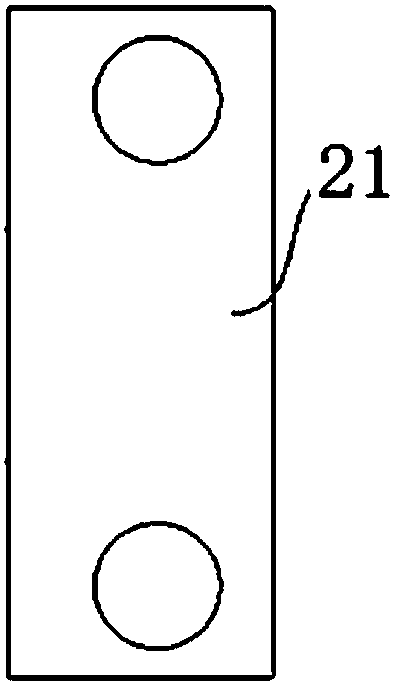
[0097] The chip testing and sealing device of present embodiment, basic structure is the same as embodiment 2, difference and improvement point are: the two ends of the enameled wire volume 111 of Hall coil and ring platform 1121 directly contact (without gasket), avoid unnecessary The magnetic field interference factor, the periphery of the enameled wire coil 111 is exposed, so as to improve the efficiency of the magnetic field. Such as Figure 7 As shown, the braiding window 22 includes a square area 221 at the bottom and a receiving area 222 at the top, and the thickness ratio of the two is 2-4:6-8. In this embodiment, the thickness ratio of the two is 3:7, and the thickness of the receiving area is relatively large. Larger, almost twice as large, providing a relatively large operating space for deviation correction; the upper surface of the pressure plate 31 is fixed with a vertical pressure plate male rail 312; the bottom surface of the bracket 32 ​​is provided with a Su...


PUM


Abstract

The invention discloses a chip testing and sealing device and a technology thereof, and belongs to the technical field of chip testing and packaging. The device comprises suction nozzles, a testing device, a lifted-leg-bagging prevention mechanism and a cover-tape-deviation prevention mechanism, and a cutter sealing mechanism, the lifted-leg-bagging prevention mechanism, the cover-tape-deviation prevention mechanism, and the cutter sealing mechanism are arranged above a carrier tape according to a process order, and the suction nozzles transfer chips tested by the testing device into the lifted-leg-bagging prevention mechanism. The lifted-leg-bagging prevention mechanism device comprises a square pressing plate and a braid window which stretches in the running direction of the carrier tapefrom the middle of the square pressing plate; an outer opening is formed in the bottom of the braid window; the cover-tape-deviation prevention mechanism comprises a pressing plate, a support and a fixed shelf; the pressing plate, the support and the fixed shelf are in soft connection in sequence; the cutter sealing mechanism comprises two sealing cutters which are parallelly arranged, a sealinggroove is formed by the two sealing cutters, and when the cutter openings of the sealing cutters are pressed, soft pressure is applied to a cover tape and the carrier tape; the vertical center lines of the braid window, a cover tape groove and the sealing groove are in the same plane to guarantee that the cover tape and the carrier tape are uniformly and tightly sealed after the chips are bagged.

Description

technical field [0001] The invention relates to the technical field of chip testing and packaging, in particular to a chip testing and sealing device and its technology. Background technique [0002] At present, in the manufacturing process of semiconductor integrated circuits, it is necessary to further test the finished chips after cutting and packaging and transfer them to the cloth bag of the carrier tape for packaging. During the testing process, the Hall coil plays the role of providing a magnetic field. [0003] Such as figure 2 As shown, the original ordinary Hall coil cannot generate a stable magnetic field in the test area, and the product parameters are easy to jump within the set range. This is because the product can only be 3mm above the coil (board Thickness 3mm) test, when adjusting the stroke of the suction nozzle, the product under the suction nozzle will move up and down in the magnetic field around the coil, and the magnetic field around the coil is extr...

Claims


Application Information

Patent Timeline
Patent Type & Authority Applications(China)
IPC IPC(8): G01R31/28H01L21/67
Inventor 李国祥汪阳胡惠民邱冬冬
Owner CHANGJIANG ELECTRONICS TECH CHUZHOU
Why Eureka
Try Eureka