Array substrate and display device
A technology of array substrate and display area, which is applied in instruments, nonlinear optics, optics, etc., can solve the problems of setting gate lines on the same horizontal line, unable to meet the wiring requirements of special-shaped display gate drive circuits, etc.
- Summary
- Abstract
- Description
- Claims
- Application Information
AI Technical Summary
Problems solved by technology
Method used
Image
Examples
Embodiment Construction
[0019] The following will clearly and completely describe the technical solutions in the embodiments of the present invention with reference to the accompanying drawings in the embodiments of the present invention. Obviously, the described embodiments are only some, not all, embodiments of the present invention. Based on the embodiments of the present invention, all other embodiments obtained by persons of ordinary skill in the art without making creative efforts belong to the protection scope of the present invention.
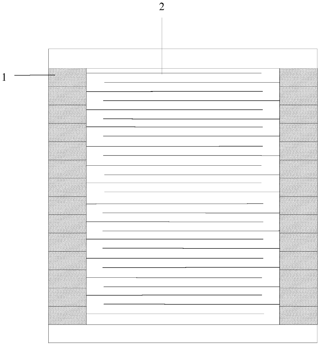
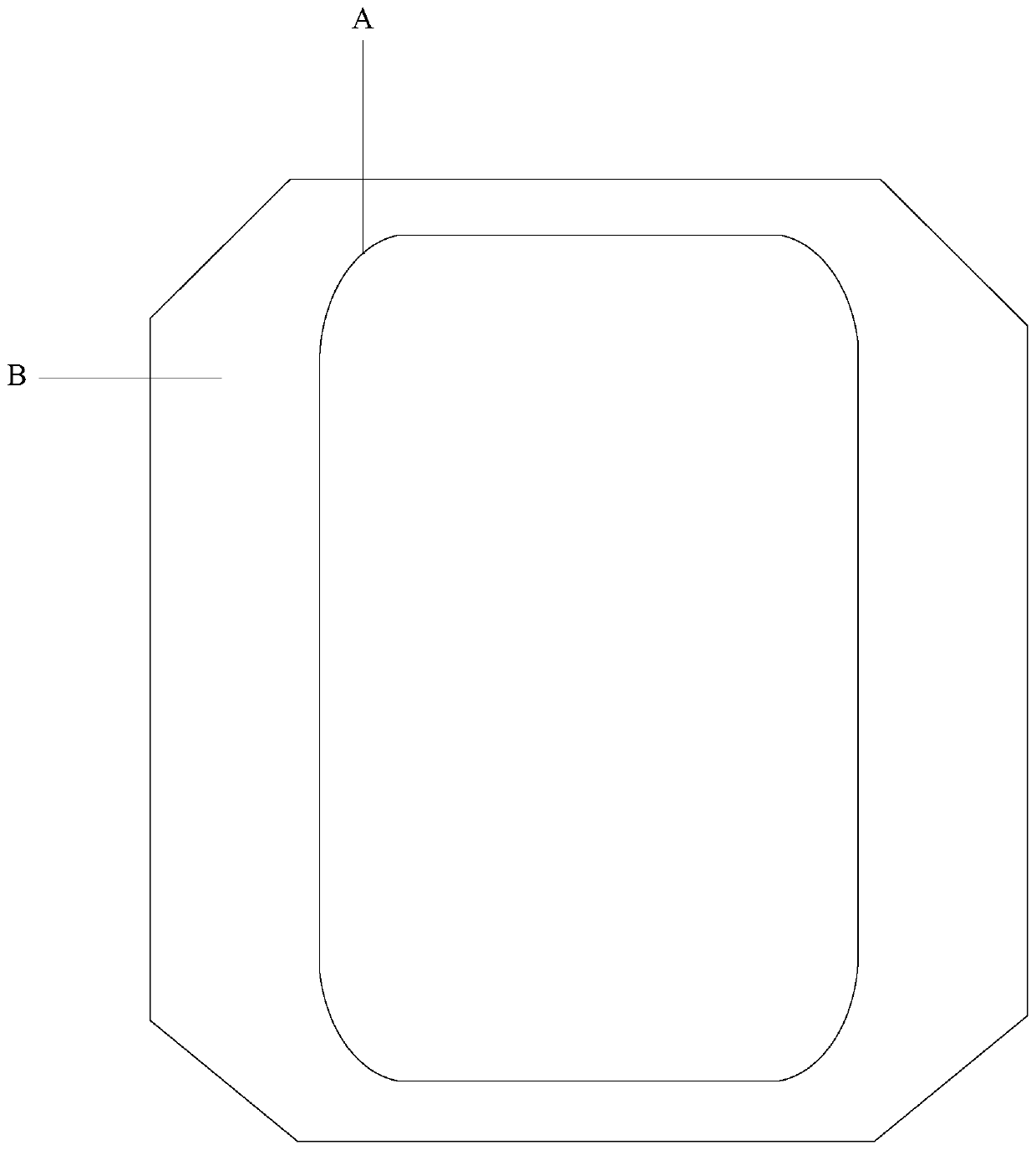
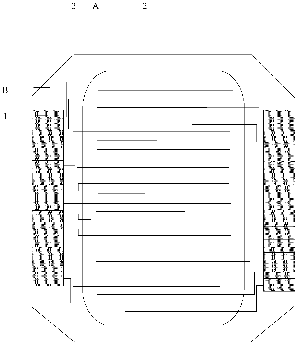
[0020] The size and shape of each component in the drawings do not reflect the real scale of the array substrate, but are only intended to schematically illustrate the content of the present invention.
[0021] Since the main improvement of the present invention lies in the gate driver part on the array substrate, when describing the embodiment of the present invention, the specific structure of the gate driver part on the array substrate is mainly introduced, ...
PUM
 Abstract
Description
Claims
Application Information


