Supercharge Your Innovation With Domain-Expert AI Agents!

Demodulator circuit and method for demodulation

A demodulator and circuit technology, applied in the field of radio frequency identification RFID technology, can solve problems such as cost increase

Active Publication Date: 2018-02-23
STMICROELECTRONICS SRL
View PDF14 Cites 6 Cited by
  • Summary
  • Abstract
  • Description
  • Claims
  • Application Information

AI Technical Summary

Problems solved by technology

[0019] Since the use of two demodulators leads to an increased cost of implementation, one of the objects of the invention is to define a single demodulator circuit and a corresponding method, which fulfill the conflicting requirements of the different standards used in HF RFID as described above

Method used


Image

  • Demodulator circuit and method for demodulation
  • Demodulator circuit and method for demodulation
  • Demodulator circuit and method for demodulation

Examples


Embodiment Construction

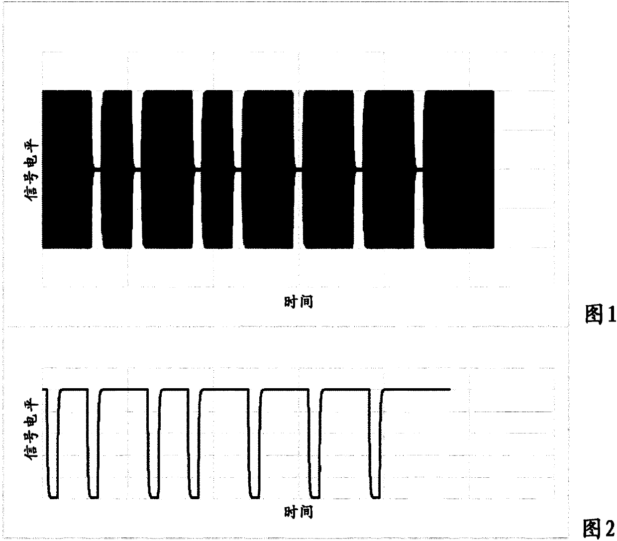
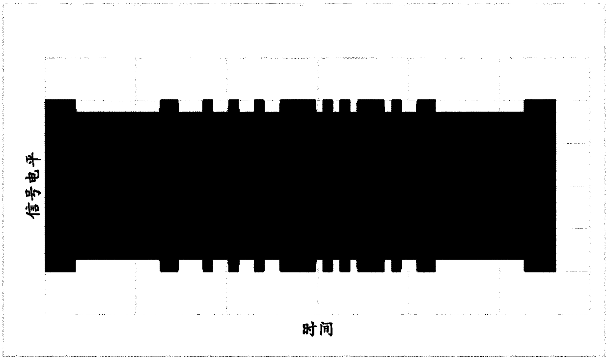
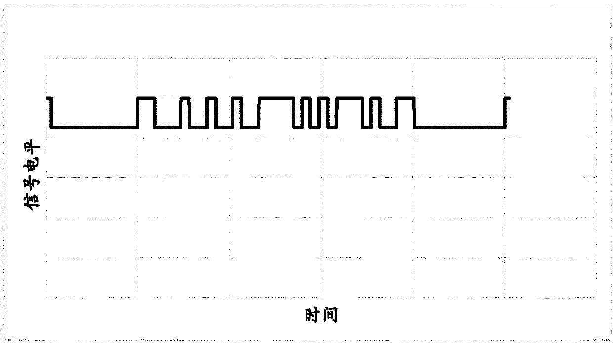
[0078] Figure 9 A first exemplary embodiment of the proposed demodulator circuit is shown. The demodulator circuit comprises an input 11 for receiving the envelope signal Senv, a unit REF for providing the switching reference signal Srefl, a filter part RC, a comparator CMP, and an output 12 for providing the output signal Sout. Cell REF is coupled to input 11 . Unit REF has an upconverter block UP, a downconverter block DWN, a first switch SW1 , a second switch SW2 and an output 9 . The filter part RC has a first variable resistor R1 and a capacitor C1. One terminal of the first variable resistor R1 is coupled to the output of the cell REF. The second terminal of the first variable resistor R1 is connected to one terminal of the capacitor C1. The other terminal of the capacitor C1 is connected to the reference potential terminal 10 . Comparator CMP has a first input 13 coupled to input 11 . The comparator CMP also has a second input 14 coupled to the output of the filt...


PUM


Abstract

The invention relates to a demodulator circuit and a method for demodulation. In one embodiment a demodulator circuit comprises an input (11) for receiving an envelope signal (Senv), a unit (REF) forproviding a switched reference signal (Sref1) at its output (9), the switched reference signal (Sref1) being provided as a function of the envelope signal (Senv) and as a function of an output signal(Sout) of the demodulator circuit, the unit (REF) being coupled to the input (11), a filter component (RC) which is connected to the output (9) of the unit (REF) for providing the switched reference signal (Sref1), the filter component (RC) being prepared to provide a filtered switched reference signal (Sref2) as a function of the switched reference signal (Sref1), and a comparator (CMP) with a first input (13) which is coupled to the input (11) of the demodulator circuit, a second input (14) which is coupled to an output of the filter component (RC) and with an output (12) for providing the output signal (Sout). The output signal (Sout) depends on a difference between the filtered switched reference signal (Sref2) and the envelope signal (Senv). A corresponding method for demodulation isspecified, as well.

Description

technical field [0001] The field of the present application is radio frequency identification RFID technology. In particular, the present application relates to demodulator circuits and methods for demodulation, in particular to the demodulation of amplitude shift keyed ASK modulated signals. Background technique [0002] The specified circuits and methods can be used in passive transponder demodulators, active transponder demodulators and near field communication NFC devices supporting peer-to-peer P2P communication mode and / or card emulation mode. [0003] ASK is the digital form of amplitude modulated AM. The modulation used in this application is ASK, but the terms AM and ASK are used interchangeably. [0004] In high frequency HF, RFID / NFC system signaling from interrogator / reader to tag or P2P, initiator to target is affected by the amplitude modulation of the carrier signal by the reader. In the case of ISO 14443B, FeliCa and ISO 15693, AM indices between 8% and 30...

Claims


Application Information

Patent Timeline
IPC IPC(8): H04L27/06H04B5/00H03D1/22H03D1/18
CPCH03D1/18H03D1/22H04L27/06H04B5/77H03D1/02H04L27/261
Inventor V·孔奇A·佩维克K·考瓦斯克
Owner STMICROELECTRONICS SRL
Features
  • R&D
  • Intellectual Property
  • Life Sciences
  • Materials
  • Tech Scout
  • Unparalleled Data Quality
  • Higher Quality Content
  • 60% Fewer Hallucinations
Learn More