A control method, device and converter for a single-inductance multi-output converter
A single-inductor multi-output, control device technology, applied in output power conversion devices, adjustment of electrical variables, control/regulation systems, etc., can solve problems such as low load capacity and large ripple
Active Publication Date: 2019-09-17
ACTIONS ZHUHAI TECH CO
5 Cites 0 Cited by
AI-Extracted Technical Summary
Problems solved by technology
The circuit structure of PFM control is relatively simple, generally adopts digital control, there is no stability prob...
Method used
Further, in the above-mentioned embodiment of the present invention, realize the control to a plurality of output (or can be understood as to the energy distribution switch control), so that energy can be added to the output branch that needs the most energy in the current clock cycle in each clock cycle, thus overcoming the problems of unbalanced load, poor transient characteristics, and serious intermodulation effects of traditional control methods shortcoming.
It can be seen that the control device of the single-inductance multi-output converter provided by the above-mentioned embodiments of the present invention, on the one hand, can realize the control of the single-inductance multi-output converter based on the PFM control mode, thereby inheriting the The PFM control method has advantages in aspects such as simple circuit structure, fast response speed, and stable circuit; at the same time, on the other hand, in each clock cycle, the only one for charging is dynamically determined according to the output voltage of each output branch. Output branches, for example, based on the hysteresis comparison results of the output voltages of each output branch for logic selection processing, so as to dynamically determine the output branch charged in each clock cycle, and the output voltage of each output branch and its load The size is closely related, so dynamically determining the output branch for charging in each clock cycle can achieve the effect of automatically adjusting the charging time of each output branch, so that the energy can be replenished in time for each output branch. At the same time, due to The output branch that is charged in each clock cycle can be selected by means of error comparison, so it can further ensure that the energy is replenished to the branch that needs the most energy in each clock cycle, so the transient response is fast and the intermodulation effect Small, and the unbalanced load of each channel basically has no influence on the circuit. Compared with the traditional single-inductance multi-output converter control scheme, it can achieve better control effects. In the loop control of the circuit, response speed, intermodulation effect, ripple Demand aspects such as waves and load imbalances have been improved.
Thus it can be seen that the control scheme provided by the above-mentioned embodiments of the present invention, on the one hand, realizes the control of the single-inductance multi-output converter based on the PFM control mode, thereby inheriting the advantages of the PFM control mode such as simple circuit structure, response Fast speed, stable circuit and other advantages; at the same time, on the other hand, the only charging output branch determined in each clock cycle is dynamically determined according to the output voltage of each output branch, and the output branch of each output branch The output voltage is closely related to the size of its load. Therefore, by dynamically determining the only output branch for charging in each clock cycle, the effect of automatically adjusting the time for each output branch to obtain charging is achieved, so it is possible to charge each output branch. The circuit can replenish energy in time, so that it can achieve better results than traditional control schemes in terms of transient characteristics and intermodulation effects. Moreover, by using the method of error comparison to determine the branch with the largest error as the output branch of charging when dynamically determining the output branch of charging in each clock cycle, the branch with the largest error can be understood as the branch that most needs supplementary energy. branches, so th...
Abstract
The invention discloses a control method, a device and a converter of a single inductance multi-output converter. The method of the present invention includes performing the following steps in each clock cycle: obtaining the output voltages of the N output branches of the single-inductance multi-output converter; selecting the clock from the N output branches according to the output voltages of the N output branches Q candidate charging branches in the cycle, Q is an integer less than or equal to N; according to the output voltage of the Q candidate charging branches, select an output branch charged in this clock cycle from the Q candidate charging branches ; According to whether the N output branches are charged in the current clock cycle, output the driving signals of the N output branches of the single-inductance multi-output converter in the current clock cycle. The invention provides a control scheme of a single-inductance multi-output converter capable of achieving better control effects.
Application Domain
Dc-dc conversionElectric variable regulation
Technology Topic
InductorVIT signals +4
Image
Examples
- Experimental program(1)
Example Embodiment
[0031] In order to make the object, technical solution and advantages of the present invention clearer, the present invention will be further described in detail below in conjunction with the accompanying drawings. Obviously, the described embodiments are only some embodiments of the present invention, rather than all embodiments . Based on the embodiments of the present invention, all other embodiments obtained by persons of ordinary skill in the art without making creative efforts belong to the protection scope of the present invention.
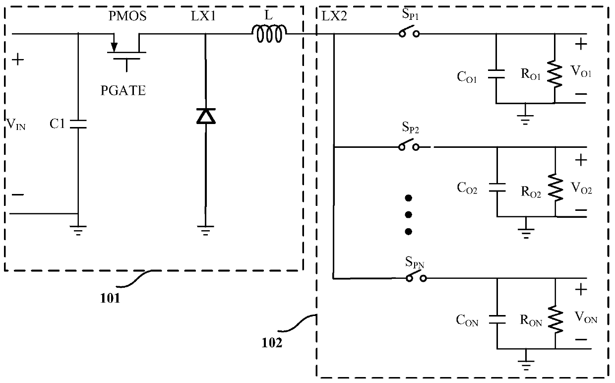
[0032] A Single Inductor Multiple Output (SIMO) converter utilizes the time-sharing working principle of each output branch, and can independently control multiple energy outputs by using one inductor. Since a plurality of output branches share one inductance, they can work in time-division, reducing the number of inductances required by the circuit, so while realizing independent control of each output branch, the size of the converter system can also be reduced.
[0033] Generally, the circuit structure of a single-inductor multiple-output converter can be divided into an energy generation part and an energy distribution part. The energy generation part can generally be the same as the circuit structure of a single-output converter, and determines the relationship between input and output voltages (such as using a boost Boost type, step-down Buck type or buck-boost Buck-Boost type, etc.), the energy distribution part generally realizes multiple outputs by setting switches in the circuit structure.
[0034] Among them, for the convenience of description, in this application, the single-inductance multi-output converter that uses a step-down Buck circuit in the energy generation part is called a single-inductance multi-output Buck converter; the energy generation part uses a boost boost converter. The single-inductor multiple-output converter of the type circuit is called the single-inductor multiple-output Boost converter; the single-inductor multiple-output converter using the buck-boost circuit for the energy generation part is called the single-inductor multiple-output Buck-Boost converter.
[0035] figure 1 A topology example of a single inductor multiple output Buck converter in the prior art is shown. like figure 1 In the shown single inductor multiple output Buck converter, the energy generation part 101 uses a P-channel Metal Oxide Semiconductor Field Effect Transistor (Positive channel Metal Oxide Semiconductor, PMOS) as the main switch, and the energy distribution part 102 uses a S P1 ,...,S PN As N energy distribution switches (or also called secondary switches), the N energy distribution switches respectively correspond to different voltage outputs of the N output branches. From such as figure 1 From the circuit structure of the single-inductor multiple-output converter, it can be seen that how to control these switches (such as the main switch and the secondary switch) so that the single-inductor multiple-output converter can generate appropriate energy and distribute the energy reasonably is a single An important part in the realization of the inductance multi-output converter circuit often needs to take into account the efficiency, stability, response rate, intermodulation effect, ripple and load capacity of the circuit.
[0036] As far as the current control methods of the single-inductance multi-output converter are concerned, there are mainly two types: PWM and PFM. Among them, most of the current research focuses on the PWM control mode, and there are relatively few studies on the PFM control mode. The PWM control method can provide greater load capacity and smaller ripple, but its loop is very complex, and its stability is difficult to analyze. It is not suitable for the situation with many output branches, and the transient response is poor, and the intermodulation effect serious. The circuit structure of the PFM control method is relatively simple, generally adopts digital control, there is no stability problem, and the response speed is fast, but its load capacity is relatively low, and the ripple is also larger than that of PWM.
[0037] Considering the various shortcomings of the traditional single-inductor multiple-output converter control methods as mentioned above, and considering the current increasing demand for low power consumption, the embodiment of the present invention provides a single-inductor multiple-output converter Converter control scheme.
[0038] In the control scheme of the single-inductor multiple-output converter provided by the embodiment of the present invention, the output voltages of the N output branches of the single-inductor multiple-output converter are obtained mainly in each clock cycle, and according to the acquired N output voltage, first determine the Q candidate charging branches in this clock cycle, and then select an output charged in this clock cycle from the Q candidate charging branches according to the output voltages of the Q candidate charging branches branches, and then according to whether the N output branches are charged in the current clock cycle, output the driving signals of the N output branches in the current clock cycle, so as to realize the control of the single inductor multiple output converter.
[0039] It can be seen that, on the one hand, the control scheme provided by the embodiment of the present invention is based on the PFM control method to realize the control of the single inductor multiple output converter, thereby inheriting the advantages of the PFM control method in aspects such as response speed and circuit stability. At the same time, on the other hand, in the control scheme provided by the embodiments of the present invention, the only output branch for charging is determined dynamically according to the output voltage of each output branch in each clock cycle, and each output branch The output voltage is closely related to the size of its load, so by dynamically determining an output branch for charging according to the output voltage of each output branch in each clock cycle, it is possible to automatically adjust the charging time of each output branch. In the case of unbalanced load, energy can be added to each output branch in a timely manner, so that better results can be achieved in terms of transient characteristics, load balance, and intermodulation effects than traditional control schemes. Therefore, comprehensively , the control scheme of the single-inductor multiple-output converter provided by the embodiment of the present invention can achieve a better control effect than the traditional control scheme of the single-inductor multiple-output converter.
[0040] Considering that the control scheme provided by the embodiment of the present invention involves the control of the single-inductor multiple-output converter, it can be applied to the circuit design of the single-inductor multiple-output converter, and can be implemented as a circuit structure, so for a clearer The control scheme of the single-inductor multiple-output converter provided by the embodiment of the present invention is described, and the control device of the single-inductor multiple-output converter provided by an embodiment of the present invention will be firstly introduced below.
[0041] figure 2 It shows a schematic structural diagram of a control device for a single-inductor multiple-output converter provided by an embodiment of the present invention. This structural example can be applied to the circuit design of a single-inductor multiple-output converter, for example, it can be specifically implemented as a single-inductor multiple-output The control stage circuit of the converter is used to control the output of the single inductor multiple output converter.
[0042] for example, figure 2 The control device of the single-inductance multi-output converter shown can be applied to such as figure 1 In the circuit design of the single-inductance multi-output Buck converter shown, through the figure 1 Based on the shown energy generation part 101 and energy distribution part 102, add as figure 2 shown in the control device, thus enabling the figure 1 Control of the single-inductor multi-output Buck converter shown.
[0043] like figure 2 As shown, the control device for a single-inductance multiple-output converter provided by an embodiment of the present invention includes: N hysteresis comparators 201 , a logic selection unit 202 and a drive unit 203 .
[0044] Specifically, such as figure 2 Of the controls shown:
[0045] N hysteresis comparators 201 are used to respectively acquire the output voltages of the N output branches of the single-inductance multi-output converter, where N is an integer greater than 1; The selection unit 202 outputs a hysteresis comparison result;
[0046] The logic selection unit 202 is configured to select Q candidate charging branches in the current clock cycle from the N output branches according to the N hysteresis comparison results output by the N hysteresis comparators 201 under the trigger of the clock cycle signal , Q is an integer less than or equal to N; and, according to the output voltages of the Q candidate charging branches, select an output branch charged in the current clock cycle from the Q candidate charging branches, and select The result is output to the drive unit 203;
[0047] The driving unit 203 is configured to output the driving signals of the N output branches of the single-inductor multiple-output converter in this clock cycle according to the selection result output by the logic selection unit 202 in each clock cycle.
[0048] Specifically, in some optional embodiments of the present invention, the N hysteresis comparators 201 are specifically used for:
[0049] Comparing the output voltage of the candidate charging branch in the last clock cycle with the first threshold, and comparing the output voltage of the non-candidate charging branch in the last clock cycle with the second threshold; wherein the first threshold is greater than the second threshold; furthermore, N level signals respectively used to indicate the N output voltage hysteresis comparison results are output to the logic selection unit 202 .
[0050] For example, in some specific embodiments of the present invention, the hysteresis comparator may be a comparator with a hysteresis loop-back transfer characteristic, with dual thresholds, a lowest threshold (equivalent to the above-mentioned second threshold) and a highest threshold Limit value (equivalent to the above-mentioned first threshold value), corresponding to the double threshold value, the hysteresis comparator can output two kinds of output level signals, which can then be used to indicate whether the output branch connected to it is a candidate charging branch or a non-charging branch. Candidate charging branch.
[0051] Among them, in the embodiment of the present invention, the candidate charging branch is used to indicate the output branch whose output voltage cannot be charged to the highest threshold value and is still in the state of charging. After the highest threshold value, it is changed to a non-candidate charging branch; correspondingly, the non-candidate charging branch is used to indicate that the output voltage has been charged to the highest threshold and enters the output branch of the discharge state. After the voltage is equal to or lower than the minimum threshold value, it is changed to a candidate charging branch.
[0052] In a specific circuit design, the N hysteresis comparators 201 can obtain the output voltages of the N output branches respectively by being respectively connected to the N output branches of the single-inductance multi-output converter. For example, the hysteresis comparators 201 can be A clock cycle is used to sample the output voltage of the output branch connected to it; and then by comparing the acquired output voltage with its own two thresholds hysteresis to obtain the output branch used to determine whether it is a candidate for charging Branch level signal.
[0053] Considering the level signal output by the hysteresis comparator, the output level signal will be relative to the last clock when the sampled output voltage drops to the lowest threshold value or the sampled output voltage rises to the highest threshold value. The output level signal of the cycle is inverted, otherwise the output level signal remains the same as the previous clock cycle. Therefore, based on the above electrical characteristics of the hysteresis comparator, in some optional embodiments of the present invention, the hysteresis comparator 201 can be specifically used for:
[0054] If the obtained output voltage rises to be greater than or equal to the first threshold, outputting a level signal for determining the output branch corresponding to the hysteresis comparator as a non-candidate charging branch;
[0055] If the obtained output voltage is reduced to be less than or equal to the second threshold, outputting a level signal for determining the output branch corresponding to the hysteresis comparator as a candidate charging branch;
[0056] Otherwise, output the same level signal as the last clock cycle.
[0057] For example, taking an output branch charged within a certain clock cycle as an example, if the hysteresis comparator 201 connected to the output branch detects that the output voltage of the output branch has risen to be higher than or equal to The highest threshold value, then output a level signal that is inverted from the previous clock cycle, that is, the level signal that indicates that the branch is a candidate charging branch is inverted to indicate that the branch is a non-candidate charging branch in this clock cycle. and the level signal indicating that the output branch is a non-candidate charging branch will be output in several subsequent clock cycles, until it is detected in a certain clock cycle that the output voltage of the branch passes through the previous When the discharge process of several clock cycles is reduced to less than or equal to the minimum threshold value, the level signal indicating that the branch is a candidate charging branch is output again by inversion; and so on.
[0058] It should be understood that, considering the electrical characteristics of the hysteresis comparator, if there is no last clock cycle, or such as considered at the initial moment, although the hysteresis comparator can output different level signals to classify an output branch as Candidate charging branches or non-candidate charging branches, for the output branches whose initial output voltage is between the first threshold and the second threshold, the states they are divided into are not fixed, but no matter whether these output branches are initially Whether it is divided into candidate charging branches or non-candidate charging branches, it can be seen that in subsequent clock cycles through the above hysteresis comparison process of the hysteresis comparator, the division of these output branches can also be gradually ordered, that is, these output The states into which branches are divided will also be deterministic. Therefore, in this application, the main focus is on the overall order, and the uncertainty that may exist at the initial moment is not considered too much.
[0059]Further, based on the N comparison results output by the N hysteresis comparators 201, the logic selection unit 202 will be able to determine the Q candidate charging branches in the current clock cycle under the trigger of the clock cycle signal, and further be able to according to For the output voltages of the Q candidate charging branches, an output branch charged in the current clock cycle is selected from the Q candidate charging branches, so as to output the selection result to the driving unit 203 for driving. Wherein, the clock period signal can be obtained by setting a circuit structure such as an oscillator in actual circuit implementation.
[0060] Specifically, in some optional embodiments of the present invention, the logic selection unit 202 is specifically configured to:
[0061] According to the results of the N output voltage hysteresis comparisons indicated by the N level signals output by the N hysteresis comparators 201, the candidate charging branches in the last clock cycle whose output voltage is not greater than the first threshold, and the output voltage is not greater than the first threshold The non-candidate charging branch in the last clock cycle greater than the second threshold is determined as the candidate charging branch in the current clock cycle.
[0062] Or it can be understood that the logic selection unit 202 acquires the N level signals output by the N hysteresis comparators 201 under the trigger of the clock cycle signal, so that it can be determined according to the N level signals The candidate charging branch of the first threshold and the non-candidate charging branch discharged to less than or equal to the second threshold in the last clock cycle are used as the candidate charging branch in the current clock cycle.
[0063] Further, in some optional embodiments of the present invention, the logic selection unit 202 may select an output branch charged in this clock cycle from the Q candidate charging branches in the following manner:
[0064] Selecting the candidate charging branch with the smallest output voltage as an output branch charged in this clock cycle, for example, the output voltages of the Q candidate charging branches can be compared with each other; or
[0065] The candidate charging branch with the largest voltage error is selected as an output branch charged in this clock cycle, wherein the voltage error of a candidate charging branch is the output voltage of the candidate charging branch and the reference voltage of the candidate charging branch the difference between. Specifically, for example, the output voltages of the Q candidate charging branches may be compared with reference voltages corresponding to the Q candidate charging branches.
[0066] Among them, compare the output voltages of the Q candidate charging branches, and select the candidate charging branch with the smallest output voltage as an output branch charged in this clock cycle, or it can also be understood as comparing the Q candidate charging branches The output voltage is the same as the reference voltage, and the candidate charging branch with the largest error between the output voltage and the reference voltage is selected as an output branch charged in this clock cycle.
[0067] It can be seen that the output branch selected by the logic selection unit 202 for charging in the current clock cycle through the above-mentioned error comparison method can also be considered as the branch that most needs to be charged in the current clock cycle. Periodically replenish the energy to the circuit that needs the most energy, so that in the case of unbalanced load of each circuit, it can also effectively reduce the impact of unbalanced load on the circuit.
[0068] In a specific circuit design, the logic selection unit 202 can be connected to N output branches, so as to sample the output voltages of the N output branches in each clock cycle, and then select the voltage from the Q candidate charging branches. The process of an output branch. Wherein, since the level signals output by the N hysteresis comparators can indicate the Q candidate charging branches in the current clock cycle, the logic selection unit 202 can first pass the logic circuit based on the level output by the N hysteresis comparators 201 The signal is converted to obtain a logic signal, so that the Q candidate charging branches are determined from the N output branches based on the converted logic signal, and the output voltages of the Q candidate charging branches are used, and then the selection circuit further performs the above-mentioned The error comparison process to realize the selection of an output branch for charging in this clock cycle.
[0069] for example, image 3 A schematic diagram of the circuit structure of an output branch used for error comparison to select charging in the control device of the single-inductance three-output converter provided by some embodiments of the present invention is shown.
[0070] It can be seen that in the image 3 The circuit structure shown includes an error generation part 301 , an error comparison part 302 and a logic conversion part 303 . Wherein, the error generating part 301 can be realized specifically by transconductance amplifiers GM1-GM3. For any output branch, the lower the output voltage is, the larger the error voltage obtained is compared with its corresponding reference voltage. The error comparison part 302 mainly compares the error signals to obtain the largest error branch EAMAX. The logic conversion part 303 is used to convert the error signal comparison signal EAMAX into a signal indicating that the branch with the largest error is the output branch for charging, for example, it can be used to indicate the sub-switch timing signals corresponding to the N branches S P1_ON ~S PN_ON , wherein the switching timing signal of the branch with the largest error is high level, which is used to enable the driving circuit to select the output branch for charging, and the rest are low level.
[0071] Another example, Figure 4 A schematic diagram of the circuit structure of an output branch used for error comparison to select charging in the control device of the single-inductance three-output converter provided by some other embodiments of the present invention is shown.
[0072] It can be seen that in the Figure 4 The circuit structure shown includes an error comparison part 401 and a logic conversion part 402 . Among them, such as Figure 4 In the circuit structure shown, it can be considered that the theoretical value (reference voltage) of the output voltage of each output branch is designed to be the same, so that the output voltage can be directly used as the error signal, and the maximum The error branch is then converted by the logic conversion part 402 into a signal for indicating that the maximum error branch is the output branch of charging, wherein the logic conversion part 402 function can be compared with image 3 The logic conversion section 303 shown is the same.
[0073] Furthermore, based on the selection result output by the logic selection unit 202 according to the determined one output branch charged in the current clock cycle, the drive unit 203 can output the current clock cycle according to whether the N output branches are charged in the current clock cycle. Driving signals of the N output branches of the single-inductor multiple-output converter.
[0074] Specifically, corresponding to the output branch determined by the logic selection unit 202 to be charged in this clock cycle, the driving signal output by the drive unit 203 is used to control the output branch to charge in the current clock cycle, corresponding to the N output Other output branches in the branches include candidate charging branches and non-candidate charging branches that are not determined to be charged, and the driving signal output by the driving unit 203 is used to control these output branches not to charge in this clock cycle .
[0075] Correspondingly, considering the circuit structure of the single-inductor multiple-output converter, in some optional embodiments of the present invention, the single-inductor multiple-output converter may specifically include a power stage circuit, and the power stage circuit is used to supply N The output branch provides energy input. for example figure 1 In the example of the single-inductance multi-output Buck converter shown, the energy generation part 101 can be understood as the power stage circuit of the single-inductance multi-output Buck converter, and the energy distribution part 102 can be understood as the single-inductance multi-output Buck converter. N output branches, wherein the energy generating part 101 is used to provide energy input to the N output branches in the energy distribution part 102 .
[0076] In some optional embodiments of the present invention, in each clock cycle, the logic selection unit 202 can also judge whether there is a candidate charging branch in this clock cycle under the trigger of the clock cycle signal, and output the judgment result to the driver Unit 203.
[0077] Considering that in some actual scenarios, the logic selection unit 202 may not be able to select the current clock cycle from the N output branches according to the N hysteresis comparison results output by the N hysteresis comparators 201 under the trigger of the clock cycle signal. Candidate charging branches, or it can be understood that the logic selection unit 202 selects the Q value of 0 in the Q candidate charging branches in this clock cycle from the N output branches, for example, when none of the N output branches The scene that needs charging is moderate. In some optional embodiments of the present invention, the logic selection unit 202 can determine whether there is a candidate charging branch in the current clock cycle based on the output results of the N hysteresis comparators 201, for example, if based on the output of the N hysteresis comparators 201 As a result, it is determined that the number of candidate charging branches in this clock cycle is 0, and the logic selection unit 202 judges that there is no candidate charging branch in this clock cycle.
[0078] Furthermore, in some optional embodiments of the present invention, when the judgment result output by the logic selection unit 202 is that there is no candidate charging branch in the current clock cycle, the output of the power stage circuit in the current clock cycle output by the drive unit 203 The driving signal is used to turn off the main switch that the power stage circuit outputs energy to the N output branches; The main switch of the road output energy.
[0079] For example, the control device of the single-inductance multiple-output converter provided by some embodiments of the present invention can be applied to such as figure 1 The single inductor multiple output Buck converter shown as an example, figure 1 The energy generation part 101 in the shown single-inductance multi-output Buck converter can be understood as the power stage circuit of the single-inductance multi-output Buck converter, and the PMOS transistor in the energy generation part 101 can be understood as the main power stage circuit. switch, when the main switch is turned on, the power stage circuit provides energy input to the N output branches in the energy distribution part 102 . If the logic selection circuit 202 determines that there is no candidate charging branch in the current clock cycle, it can be considered that the N output branches have all completed a complete charging process, and enter the discharge stage. Before the second threshold, charging will no longer be carried out, so the determination result output by the logic selection circuit 202 will make the drive unit 201 control the PMOS transistor in the energy generating part 101 to turn off, otherwise, if there is at least one candidate charging branch, then it can be considered Currently at least one output branch needs to be charged, so the determination result output by the logic selection circuit 202 will make the driving unit 201 control the PMOS transistor in the energy generating part 101 to turn on to provide energy input to the output branch.
[0080] Correspondingly, in some optional embodiments of the present invention, the power stage circuit of the single-inductor multiple-output converter may be specifically connected to N output branches through N sub-switches. for example figure 1 In the example of the single-inductance multi-output Buck converter shown, the energy generation part 101 can be understood as the power stage circuit of the single-inductance multi-output Buck converter, and the energy distribution part 102 can be understood as the single-inductance multi-output Buck converter. N output branches, wherein, the energy generating part 101 passes through N sub-switches (S P1 ,...,S PN ) are respectively connected to N output branches.
[0081] Furthermore, in some optional embodiments of the present invention, in each clock cycle, the drive unit 203 may specifically output the output branch for turning on the output branch charged in this clock cycle according to the selection result output by the logic selection unit 202 The driving signal of the sub-switch corresponding to the branch; for the output branch that does not charge in the current clock cycle, output the driving signal for turning off the sub-switch corresponding to the output branch.
[0082]It can be seen that the control device for the single-inductor multiple-output converter provided by the above-mentioned embodiments of the present invention, on the one hand, can realize the control of the single-inductor multiple-output converter based on the PFM control mode, thereby inheriting the PFM control mode Advantages in aspects such as simple circuit structure, fast response, stable circuit, etc.; at the same time, in each clock cycle, the only output branch for charging is dynamically determined according to the output voltage of each output branch , for example, based on the hysteresis comparison results of the output voltage of each output branch, the logic selection process is carried out, so as to dynamically determine the output branch charged in each clock cycle, and the output voltage of each output branch is closely related to the size of its load. , thus dynamically determining the output branch for charging in each clock cycle can achieve the effect of automatically adjusting the charging time of each output branch, so that the energy can be replenished for each output branch in time, and because the error can be taken The comparison method selects the output branch that is charged in each clock cycle, so it can further ensure that the energy is replenished to the branch that needs the most energy in each clock cycle, so the transient response is fast and the intermodulation effect is small. The circuit load imbalance basically has no effect on the circuit. Compared with the traditional single-inductance multi-output converter control scheme, it can achieve better control effect. In the loop control of the circuit, response speed, intermodulation effect, ripple and load The demand side, such as imbalance, has been improved.
[0083] In order to more clearly explain the control device of the single-inductance multiple-output converter provided by the above-mentioned embodiments of the present invention and the control scheme provided by the embodiments of the present invention, some implementations of the present invention will be described below in conjunction with specific circuit implementations An example of the application of the control device of the single-inductance multi-output converter provided in the example in the actual scene.
[0084] Figure 5 A schematic circuit structure diagram of a single-inductance multiple-output Buck converter applying the control scheme of the single-inductance multiple-output converter provided by some embodiments of the present invention is shown.
[0085] like Figure 5 As shown, the single inductor multiple output Buck converter includes a power stage circuit 501 , N output branches 502 and a control stage circuit 503 . Wherein, the control stage circuit 503 can be regarded as a specific circuit implementation example of the control device of the single-inductance multiple-output converter provided in some embodiments of the present invention in this scenario.
[0086] Specifically, such as Figure 5 As shown, the power stage circuit 501 and the N output branches 502 respectively correspond to two parts of energy generation and energy distribution. In this specific application example, a PMOS transistor is used as a main switch in the power stage circuit 501, and an NMOS transistor is used as a synchronous rectifier transistor; N output branches pass through N secondary switches (such as Figure 5 S shown P1 ~S PN ) is connected to the power stage circuit; the control stage circuit 503 includes N hysteresis comparators (such as Figure 5 The shown CMP1~CMPN) 5031, and the logic selection unit 5032 composed of an oscillator, a maximum error detection circuit, and a logic circuit, and a driving unit 5033 including a main driving circuit and a secondary driving circuit; wherein, in the logic selecting unit 5032 The oscillator is used to provide clock signals for the logic circuit and the maximum error detection circuit in the logic selection unit 5032; in addition, in this specific application example, the control stage circuit 503 also adaptively includes a circuit for providing current protection for the PMOS tube The peak current limit 5034, the peak current limit 5034 obtains the current at the PMOS tube, and provides an input to the logic selection unit 5032, so that when the logic selection unit 5032 determines that the PMOS tube needs to be turned on according to the hysteresis comparison result, it can ensure that the POMS tube When the current at the point reaches the current limit point, it can control the PMOS tube to turn off.
[0087] Specifically, the turn-on or turn-off of the main switch PMOS in the power stage circuit 501 as the energy generation part can be controlled by the main drive circuit in the drive unit 5033 according to the output of the logic circuit in the logic selection unit 5032 (such as Figure 5 PGATE pulse timing drive signal shown), and because the synchronous rectifier NMOS in the power stage circuit 501 is used for synchronous rectification, when the main drive circuit in the drive unit 5033 controls the PMOS to turn off, it can also control the NMOS to turn on (like Figure 5 NGATE pulse timing drive signal shown); N sub-switches (S P1 ~S PN ) are turned on or off, and can be controlled by the secondary drive circuit in the drive unit 5033 according to the output of the maximum error detection circuit in the logic selection unit 5032 (such as Figure 5 The N sub-switches shown (S P1 ~S PN ) pulse timing drive signal).
[0088] Specifically, such as Figure 5 As shown, the hysteresis comparators CMP1-CMPN in the control stage circuit 503 are used to implement the hysteresis control function on the output voltage. For example, taking any output branch as an example, it is assumed that the output branch is initially (assuming that the corresponding secondary switch is S PX ) output voltage below the threshold voltage V REFX_L (equivalent to the second threshold), the hysteresis comparator will output a high level, and after logic control, it will turn on the sub-switch S corresponding to the output branch PX to charge the output branch until the output voltage of the output branch is higher than the threshold voltage V REFX_H (equivalent to the first threshold), the hysteresis comparator outputs a low level, and the secondary switch S corresponding to the output branch will be disconnected after logic control PX , thereafter the output load is provided by the load capacitor until the output voltage drops to V REFX_L When , the output of the hysteresis comparator flips to a high level again, repeating the previous process.
[0089] Further, as Figure 5 As shown, the logic selection unit 5032 in the control stage circuit 503 processes the output control signals VC1~VCN of the hysteresis comparators through a logic circuit. On the one hand, the logic circuit in the logic selection unit 5032 will base Whether the branch exists) and the input (OCP) from the peak current limiter 504 controls the main drive circuit to drive the main switch PMOS tube and the synchronous rectification NMOS tube output in the power stage circuit 501 accordingly, and on the other hand will process The result (for example, logic signals corresponding to the determined Q candidate charging branches) is input to the maximum error detection circuit in the logic selection unit 5032 to further determine an output branch for charging in this clock cycle.
[0090] for example Figure 5 As shown, the PMOSON signal output by the logic circuit in the logic selection unit 5032 to the main drive circuit in the drive unit 5033 corresponds to the switching timing of the main switch PMOS tube, and when it is high, it means that the main switch PMOS tube is turned on, and the NMOSON signal Corresponding to the switching sequence of the synchronous rectification NMOS tube, when it is high, it means that the synchronous rectification NMOS tube is turned on; the logic circuit in the logic selection unit 5032 outputs the PFM1ON~PFMNON signals to the maximum error detection circuit respectively corresponding to V O1 ~V ON When it is high, it means that the output branch corresponding to the signal needs to be charged (that is, it is a candidate charging branch);
[0091] Furthermore, when the maximum error detection circuit detects the maximum error branch, it limits the detection range to Q output branches (candidate charging branches) that need to be charged from the output voltages of the N output branches according to the instructions of PFM1ON~PFMNON , where, in such as Figure 5 In the maximum error detection circuit shown, the theoretical values (i.e., reference voltages) of each output branch are designed to be equal, so the error signal can be directly represented by the feedback output voltage signal. In some examples, each output branch in the maximum error detection circuit The reference voltages of the circuits are not exactly equal, so the error signal can also be a differential amplification signal of the feedback output voltage signal and the reference voltage. Specifically, the control signal of the sub-switch corresponding to the maximum error branch (an output branch of charging) detected by the maximum error detection circuit will become a high level, and the control signals of the sub-switches corresponding to the remaining output branches will be low. flat. The sub-drive circuit in the drive unit 5033 is used to convert the logic control signal (S P1_ON ~S PN_ON ) into a drive signal (S P1 ~S PN ), and generate a corresponding dead time for the driving signals of the sub-switches corresponding to each output branch, so as to prevent overlap and collusion of the sub-switches.
[0092] Image 6 A schematic circuit structure diagram of a single-inductance multiple-output Boost converter applying the control scheme of the single-inductance multiple-output converter provided by some embodiments of the present invention is shown.
[0093] Among them, due to Image 6 The illustrated single-inductance multiple-output Boost converter applying the control scheme of the single-inductance multiple-output converter provided by some embodiments of the present invention and Figure 5 Compared with the single-inductance multiple-output Buck converter that applies the control scheme of the single-inductance multiple-output converter provided by some embodiments of the present invention, only the specific circuit structure and electrical characteristics of the power stage circuit are different. , which respectively correspond to the Boost type and the Buck type, and do not affect the application of the control device for the single-inductance multi-output converter provided by the embodiment of the present invention, so the Image 6 The specific description of the circuit design can refer to the previous Figure 5 The illustrated description of the single-inductor multiple-output Buck converter applying the control scheme of the single-inductor multiple-output converter provided by some embodiments of the present invention will not be repeated here.
[0094] Further, in the above-mentioned embodiments of the present invention, through the hysteresis comparison of the hysteresis comparator and the selection process of the logic selection unit, each output branch is in the candidate charging state, the charging state and the non-candidate charging state in each clock cycle. , where the charging process can be considered as an intermediate state of each output branch state change, accompanied by the respective charging and discharging process, it can be considered that at the end of each clock cycle, the state of each output branch is between the candidate charging state and the non-candidate charging state Therefore, logically, the state change of each output branch in the control scheme of the single inductor multiple output converter provided by the embodiment of the present invention can also be understood as a mechanism of a state machine.
[0095] In order to more clearly illustrate the working mechanism of the control scheme of the single-inductance multiple-output converter provided by some embodiments of the present invention from a logical level, Figure 7 A flowchart of a state machine corresponding to a single-inductance three-output converter applying the control scheme provided by some embodiments of the present invention is shown.
[0096] like Figure 7 As shown, assume that the state bits obtained after the three output branches of the single-inductance three-output converter pass through the logic circuit in the logic selection unit represent the states of PFM3ON, PFM2ON, and PFM1ON in sequence from high to low. When PFMiON is 0 It means that the i-th output branch does not need to be charged (non-candidate charging branch), and when PFMiON is 1, it means that the i-th output branch needs to be charged (candidate charging branch), and i is 1, 2 or 3; for example, 001 means 3rd output branch V O3 with the 2nd output branch V O2 No need to charge, the first output branch V O1 Need to recharge.
[0097] like Figure 7 As shown, it can be seen that any state in the state machine can jump to another state in the state machine through a certain change process, so it can theoretically start from any state at the beginning. Assuming an initial state of 111 in an example, V O1 , V O2 and VO3 are required to be charged, so first from V O1 , V O2 and V O3 The path with the largest detected error is charged. After one clock cycle, if V O1 , V O2 and V O3 If it is still less than the set maximum threshold, the maximum error detection is performed again, and the previous process is repeated. It can be considered that the state machine fails to reach the state jump condition in this process. . Suppose at this time V O1V REF1_H , where V REF1_H means V O1 Correspondingly set the highest threshold (the first threshold), then the state machine jumps to the 110 state, at this time V O1 The corresponding output branch will not need charging (non-candidate charging branch), so the V O2 and V O3 The maximum error branch determined in is charged, and the cycle detection and charging are carried out continuously. During this process, the following three situations will occur: If V O2V REF2_H , where V REF2_H means V O2 Correspondingly set the highest threshold, then the state machine jumps to the 100 state; if V appears first O3V REF3_H , where V REF3_H means V O3 Correspondingly set the highest threshold, then the state machine jumps to the 010 state; and if V O1 REF1_L , where V REF1_L means V O1 Correspondingly set the lowest threshold (the second threshold), then the state machine will return to the 111 state. After entering other states, the state machine performs the same operation as the above state jump.
[0098] It can be seen that for a single-inductor three-output converter, such as Figure 7 The state machine shown includes all possible states, and each state corresponds to a clear operation and state transition, so it can be seen that the state machine based on the control scheme provided by the embodiment of the present invention is implemented The state control is complete, and there will be no state omission and dead loop on the logic level, so the reliability of the single-inductance multi-output converter control can be guaranteed in the control.
[0099] Further, in the above-mentioned embodiments of the present invention, the control of multiple outputs (or it can be understood as the control of the energy distribution switch) is realized through the hysteresis comparison of the hysteresis comparator and the selection process based on the error comparison of the logic selection unit. , so that energy can be added to the output branch that needs the most energy in the current clock cycle in each clock cycle, thus overcoming the shortcomings of traditional control methods such as unbalanced load, poor transient characteristics, and serious intermodulation effects.
[0100] In order to more clearly illustrate the advantages of the single-inductance multiple-output converter control scheme provided by some embodiments of the present invention in terms of load balance, transient characteristics, and intermodulation effects, the following will combine Figure 8 , Figure 9 and Figure 10 The timing diagrams of the output voltages of the single-inductor three-output converters in different scenarios to which the control solutions of the single-inductor multiple-output converters provided by some embodiments of the present invention are respectively shown are described.
[0101] Figure 8 Shown is a timing diagram of output voltages of a single-inductance three-output converter applying the control scheme provided by some embodiments of the present invention in a load unbalanced scenario.
[0102] where, assuming V O1 The branch load is light, V O3 Branches are heavily loaded. like Figure 8 As shown, at t1, V is detected O1 REF1_L , so it is first charged for one clock cycle (S p1 is high); at t2, V is detected O2 REF2_L and V O2 The error is large (EA2>EA1), so to V O2 Charge for one clock cycle (S p2 is high); at t3, V is detected O3 REF3_L And EA3>EA2>EA1, so to V O3 Charge for one clock cycle (S p3 is high level); at t4, it is detected that EA3 is still the maximum, so it continues to V O3 Charging (S p3 is high level); at t5, EA2>EA3>EA1 is detected, and thus to V O2 Charge for one clock cycle. So work until t6, V O1V REF1_H , so V O1 will not require charging, so the next clock cycle maximum error is only at V O2 with V O3 to choose from. to t7, due to V O2V REF2_H , so V O2 There will also be no charging required, thus leaving only V O3 until charged to V REF3_H. It can be seen that during the whole process, due to V O1 The load is lighter and thus will reach the highest threshold voltage first, at V O1 down to V REF1_L Before its energy distribution switch (V O1 The corresponding secondary switch) will not be turned on again, and the maximum error detection is only at V O2 and V O3 in, so it will not affect the other two outputs; V O3 The load is the heaviest, so the highest threshold voltage is reached at the end, and it will not affect the output of the other two. Therefore, it can be seen that the scene of unbalanced load will not affect the control effect of the control scheme provided by the embodiment of the present invention on the single-inductance multi-output converter, that is, the control scheme provided by the embodiment of the present invention can be very good It is suitable for application scenarios with unbalanced load.
[0103] based on Figure 8 shown in the timing diagram, further, Figure 9 The timing diagram of the output voltage of the single-inductance three-output converter applied with the control scheme provided by some embodiments of the present invention is changed from light load to heavy load.
[0104] where, assuming V O1 The load suddenly jumps from light load to heavy load. like Figure 9 shown, at V O1 When the load suddenly jumps from light load to heavy load, the current charging V O1 The rising rate of the output voltage will be slower, and the falling rate will be faster in the uncharged clock cycle, but because the error comparison method is used to determine the charging output branch in each clock cycle (equivalent to the secondary Energy allocation using the error comparison method), so in the V O1 When the faster speed drops to a certain value, it will be judged as the largest error branch due to the mechanism of determining the output branch of charging due to its error comparison, so it will be charged again, so that the output voltage will gradually increase, and it can be seen that due to the whole process Due to the use of digital signal control, the response speed is very fast, V O1 The output voltage of the output voltage will not have a large undershoot, and the transient characteristics are better; and for the other two branches where the load does not change, it only takes longer to rise to the highest threshold, and will not affect the ripple. The size of the wave, so the intermodulation effect has basically no influence.
[0105] based on Figure 8 shown in the timing diagram, further, Figure 10 It shows a sequence diagram of the output voltage of the single-inductance three-output converter applying the control scheme provided by some embodiments of the present invention under the scenario of jumping from heavy load to light load.
[0106] where, assuming V O3 The load suddenly jumps from heavy load to light load. like Figure 10 shown, at V O3 When the load suddenly changes from heavy load to light load, the current discharged V O3 The fall rate will be slower, and the rise rate will be faster during the clock cycle when it gets charged, such as Figure 10 shown, V O3 rises to the highest threshold V by subsequent charging in only one clock cycle REF3_H , thereafter at V O3 falls to the minimum threshold V REF3_L Before, it will not be cycled and will not participate in the maximum error detection, so V O3 The output voltage of the output voltage will not have a large overshoot, and the transient characteristics are better; and for the other two branches where the load does not change, it only shortens the time to rise to the highest threshold, which will also not affect the ripple. The size of the wave, so the intermodulation effect has basically no influence.
[0107] It can be seen from the above description that in the control scheme of the single-inductor multiple-output converter provided by the above-mentioned embodiments of the present invention, the output control of the single-inductor multiple-output converter is realized through the following steps in each clock cycle, including First obtain the output voltages of the N output branches of the single-inductance multi-output converter, and first determine the Q candidate charging branches in this clock cycle according to the obtained N output voltages. The output voltage of the branch is compared with hysteresis; and then an output branch charged in this clock cycle is selected from the Q candidate charging branches, for example, it is realized by comparing the output voltages of the Q candidate charging branches. ; Further, according to whether the N output branches are charged in the current clock cycle, output the driving signals of the N output branches in the current clock cycle.
[0108] Therefore, it can be seen that the control scheme provided by the above-mentioned embodiments of the present invention, on the one hand, realizes the control of the single-inductance multi-output converter based on the PFM control method, thereby inheriting the advantages of the PFM control method such as simple circuit structure, fast response speed, circuit stability and other advantages; at the same time, on the other hand, the only charging output branch determined in each clock cycle is dynamically determined according to the output voltage of each output branch, and the output voltage of each output branch is It is closely related to the size of its load, so by dynamically determining the only output branch for charging in each clock cycle, the effect of automatically adjusting the time for each output branch to obtain charging is achieved, so that each output branch can be timely Supplement energy, so that it can achieve better results than traditional control schemes in terms of transient characteristics and intermodulation effects. Moreover, by using the method of error comparison to determine the branch with the largest error as the output branch of charging when dynamically determining the output branch of charging in each clock cycle, the branch with the largest error can be understood as the branch that most needs supplementary energy. branches, so that energy can be supplemented to the most energy-requiring branches in each clock cycle, which overcomes the shortcomings of traditional methods such as unbalanced load, poor transient characteristics, and serious effects of intermodulation effects; at the same time, through the above-mentioned It can also be seen from the description of the state machine provided by the embodiment that the control scheme provided by the embodiment of the present invention takes into account various situations of branch outputs, so the reliability is good. Taken together, the control scheme of the single-inductor multiple-output converter provided by the above-mentioned embodiments of the present invention is better than the control scheme of the traditional single-inductor multiple-output converter in terms of load balancing, transient characteristics and intermodulation effects. And many other aspects have been comprehensively optimized to achieve better control effects.
[0109]For example, analysis of the practice of charging the output voltage to the highest threshold successively in some existing technical solutions shows that if the load of the front-stage branch is heavy, it will cause the rear-stage branch to wait for a long time for charging. And if the load of the subsequent branch circuit is also heavy, the lowest value drops very seriously, which will further lead to a very large ripple, which will be amplified step by step, and the ripple of the last stage may exceed the margin of the circuit. In addition, when the front branch suddenly changes from light load to heavy load, the waiting time for the subsequent branch will also increase, which is manifested as intermodulation effect, and each branch has the influence of intermodulation effect. The ripple of each branch meets the design requirements, and the load capacity will be very small, but the load capacity that is too low often cannot meet the requirements of the maximum instantaneous load. However, the control scheme of the single-inductance multiple-output converter provided by the embodiment of the present invention is equivalent to dynamically determining the output branch of charging in each clock cycle, so the turn-on time of each branch can be automatically adjusted according to the size of the load, thereby It can replenish energy to the branch that needs the most energy in each clock cycle, and the unbalanced load of each circuit has basically no effect on the circuit. It has many advantages such as fast transient response and small intermodulation effect.
[0110] Furthermore, compared with the existing technical scheme, the control scheme of the single inductor multiple output converter provided by the embodiment of the present invention can not only supply energy to the most needed output branch in each clock cycle, but also because the whole The process adopts digital signal control, so it can better adapt to the scene of unbalanced load and load change, with faster response speed and better transient characteristics, and can be applied to the circuit design of various single-inductance multi-output converters , not limited to application scenarios, and easy for product implementation.
[0111] To sum up, the control scheme of the single-inductor multiple-output converter provided by the embodiment of the present invention, compared with the control scheme of the traditional single-inductor multiple-output converter, not only can inherit the simple structure of the PFM control method , fast response, no stability problems, etc., can also dynamically determine the charging output branch in each clock cycle, so that energy can be supplemented to the branch that needs the most energy, and can automatically adjust each branch according to the size of the load. The charging time of the branch circuit is obtained, so the transient response is fast, the intermodulation effect is small, and the load imbalance of each circuit basically has no effect on the circuit, so that the circuit can improve efficiency, stability, response rate, intermodulation effect, ripple and Compared with the traditional method, the load capacity and other aspects have been improved.
[0112] Based on the same technical idea, an embodiment of the present invention also provides a control method for a single-inductance multi-output converter, the flow of the method can be executed by the single-inductance multi-output converter provided in any of the above embodiments, and the flow of the method can be applied to In the circuit design of the single-inductor multi-output converter, it can be implemented as a control stage circuit to realize the control of the single-inductor multi-output converter.
[0113] Figure 11 A schematic flowchart of a control method for a single-inductance multiple-output converter provided by some embodiments of the present invention is shown.
[0114] Specifically, such as Figure 11 As shown, the method flow includes executing a control process for the single-inductance multiple-output converter in each clock cycle, and the control process may include the following steps:
[0115] Step 1101: Obtain the output voltages of N output branches of the single-inductor multiple-output converter, where N is an integer greater than 1;
[0116] Step 1102: According to the output voltages of the N output branches, select Q candidate charging branches in the current clock cycle from the N output branches, where Q is an integer less than or equal to N;
[0117] Step 1103: According to the output voltages of the Q candidate charging branches, select an output branch charged in the current clock cycle from the Q candidate charging branches;
[0118] Step 1104: According to whether the N output branches are charged in the current clock cycle, output the driving signals of the N output branches of the single inductor multiple output converter in the current clock cycle.
[0119] Specifically, in some optional embodiments of the present invention, after the output voltages of the N output branches of the single-inductance multiple-output converter are obtained through step 1101, the Q output voltages described in step 1102 in this clock cycle are determined Candidate charging branches can be implemented in the following ways:
[0120] Comparing the output voltage of the candidate charging branch in the last clock cycle with the first threshold, and comparing the output voltage of the non-candidate charging branch in the last clock cycle with the second threshold; wherein the first threshold is greater than the second threshold; and then according to the comparison result, select Q candidate charging branches in the current clock cycle from the N output branches.
[0121] In some optional embodiments of the present invention, specifically, the candidate charging branches in the last clock cycle whose output voltage is not greater than the first threshold, and the non-candidate charging branches in the last clock cycle whose output voltage is not greater than the second threshold The charging branch is determined as a candidate charging branch in this clock cycle.
[0122] For example, for an output branch charged in the last clock cycle, if its output voltage is greater than or equal to the first threshold, the branch is changed to a non-candidate charging branch in this clock cycle; otherwise, the branch is still charged. Determined as the candidate charging branch in this clock cycle; for the candidate charging branch that was not charged in the last clock cycle, it is still determined as the candidate charging branch in this clock cycle; for the non-candidate charging branch in the last clock cycle , if the output voltage thereof is less than or equal to the second threshold, the branch is changed to a candidate charging branch in this clock cycle.
[0123] Further, in some optional embodiments of the present invention, after the Q candidate charging branches in the current clock cycle are determined through step 1102, the current clock is selected from the Q candidate charging branches described in step 1103 An output branch for charging within a cycle, specifically, select the candidate charging branch with the smallest output voltage as an output branch for charging in this clock cycle; or select the candidate charging branch with the largest voltage error as the output branch for charging in this clock cycle. An output branch of charging, wherein the voltage error of a candidate charging branch is the difference between the output voltage of the candidate charging branch and the reference voltage of the candidate charging branch.
[0124] In order to more clearly describe the process of determining an output branch charged in the current clock cycle from N output branches in some embodiments of the present invention, Figure 12 From the logic level, it shows a schematic diagram of the logic flow of determining an output branch charged in the current clock cycle from N output branches in some embodiments of the present invention.
[0125] in such as Figure 12 In the flow shown, three databases are defined to logically classify the output voltages of each output branch. Among them, for the convenience of description, in the image 3 In the logic flow shown, a kind of processing at the initial moment is logically assumed, which includes the initial moment, and it can be considered that the output voltages of all output branches (assuming V O1 ,...,V ON Indicates) are placed in the Z library; pass and the first threshold (assuming V REFH denoted) in two parts: X bank and Y bank; where all output voltages are less than V REFH The output branch of X is placed in the X library (assuming that the output branch in the X library uses V O(p1) …V O(pn) indicated), all output voltages are not less than V REFH The output branch of is placed in the Y bank (assuming that the output branch in the Y bank uses V O(q1) …V O(qm) represents), where N=n+m.
[0126] like image 3 As shown, the output branches in the X library can be considered as candidate charging branches, so in each clock cycle, one of the output branches will be selected through mutual comparison (which can be understood as the aforementioned error comparison process). The road is used as the output branch charged in the current clock cycle, such as image 3 As shown, by taking the error voltage between the output voltage of the output branch in the X library and the reference voltage (assumed to be expressed as EA (p1) …EA (pn) ), select the branch EA with the largest error (X)max (X=p X ), so that the output branch is charged in the current clock cycle. The output voltage of this output branch after charging V OX will again be set with the highest threshold V REFH compared if less than V REFH , it still belongs to the X library, that is, it is still a candidate charging branch, and enters the selection cycle of the output branch of the next charge; if it is greater than or equal to V REFH , then the output branch is classified into the Y library, and the output branch in the Y library is a branch that does not charge, that is, it can be considered as a non-candidate charging branch, and the load current is provided by the load capacitance, so its output voltage will drop, and when a certain branch voltage V in the Y bank OY drops to less than V REFL , it means that the branch needs to be charged, so the branch is placed in the X library and participates in the maximum error detection process to determine whether to charge. After one clock cycle ends, the remaining branches in the X bank will perform the next cycle in the next clock cycle, and the branches in the Y bank will not be charged. It should be understood that the above-mentioned processing at the initial moment is a logical assumption, but each output branch will be gradually ordered through the process of charging and discharging and the processing in subsequent clock cycles (in the X bank or Y library), so the uncertainty that may exist at the initial moment is not considered too much in this application.
[0127] In some optional embodiments of the present invention, the single-inductor multiple-output converter may specifically include a power stage circuit, and the power stage circuit is used to provide energy input to the N output branches.
[0128] Furthermore, in some optional embodiments of the present invention, in each clock cycle, it can also be judged whether there is a candidate charging branch in the current clock cycle, so that according to whether there is a candidate charging branch in the current clock cycle, output The driving signal of the power stage circuit of the single inductor multiple output converter is used to control whether the power stage circuit of the single inductor multiple output converter provides energy input to the output branch.
[0129] In some optional embodiments of the present invention, if there is no candidate charging branch in this clock cycle, then output the main charging circuit used to turn off the power stage circuit to output energy to the N output branches in this clock cycle. a driving signal of a switch; otherwise, outputting a driving signal of a main switch used to turn on the power stage circuit to output energy to the N output branches in this clock cycle.
[0130] In some optional embodiments of the present invention, the power stage circuit of the single-inductor multiple-output converter may be respectively connected to N output branches through N sub-switches.
[0131] Furthermore, in some optional embodiments of the present invention, in each clock cycle, according to whether the N output branches described in step 204 are charged in the current clock cycle, the output of the single inductor multiple output converter in the current clock cycle is output The driving signals of the N output branches can specifically be to output the driving signal for turning on the sub-switch corresponding to the output branch for the output branch charged in the current clock cycle; for the output branch that is not charged in the current clock cycle , outputting a driving signal for turning off the secondary switch corresponding to the output branch.
[0132] Wherein, the control method of the single-inductance multiple-output converter provided by the above-mentioned embodiments of the present invention can be referred to the control device of the single-inductor multiple-output converter provided by the above-mentioned embodiments of the present invention in the specific circuit implementation. This will not be repeated.
[0133] Based on the same technical idea, an embodiment of the present invention also provides a single-inductance multiple-output converter, which includes a power stage circuit and the A control device, the control device can be used to implement the aforementioned method embodiments.
[0134]Wherein, the power stage circuit is respectively connected to N output branches through N sub-switches; N is an integer greater than 1; the control device is used to select an output branch charged in this clock cycle in each clock cycle, and output this The driving signals of the N output branches of the single-inductor multiple-output converter in a clock cycle are used to drive the N sub-switches to be turned on or off.
[0135] Wherein, for the control device in the single-inductance multiple-output converter provided by some optional embodiments of the present invention, reference may be made to the foregoing description of the control device of the single-inductance multiple-output converter provided by the embodiment of the present invention. No further details will be given.
[0136] In some optional embodiments of the present invention, the power stage circuit may be a step-down Buck circuit, and a main switch PMOS transistor is arranged in the step-down Buck circuit;
[0137] The control device is also used to: in each clock cycle, judge whether there is a candidate charging branch in this clock cycle; if there is no candidate charging branch in this clock cycle, then output The drive signal of the main switch PMOS tube; otherwise, output the drive signal used to turn on the main switch PMOS tube in this clock cycle.
[0138] Specifically, for the single-inductance multiple-output converter using a step-down Buck circuit as a power stage circuit provided by some optional embodiments of the present invention, please refer to the foregoing Figure 5 The schematic diagram of the circuit structure of the single-inductance multiple-output Buck converter applying the control scheme of the single-inductance multiple-output converter provided by some embodiments of the present invention and related descriptions are shown, and this application will not repeat them here. .
[0139] In some optional embodiments of the present invention, the power stage circuit is a boost boost circuit, and a main switch NMOS transistor is arranged in the boost boost circuit;
[0140] The control device is also used to: in each clock cycle, judge whether there is a candidate charging branch in this clock cycle; if there is no candidate charging branch in this clock cycle, then output The drive signal of the main switch NMOS tube; otherwise, output the drive signal used to turn on the main switch NMOS tube in this clock cycle.
[0141] Specifically, for the single-inductance multiple-output converter using a step-down Buck circuit as a power stage circuit provided by some optional embodiments of the present invention, please refer to the foregoing Image 6 The schematic diagram of the circuit structure of the single-inductor multiple-output Boost converter applying the control scheme of the single-inductor multiple-output converter provided by some embodiments of the present invention and related descriptions will not be repeated in this application. .
[0142] The present invention is described with reference to flowchart illustrations and/or block diagrams of methods, apparatus (systems), and computer program products according to embodiments of the invention. It should be understood that each procedure and/or block in the flowchart and/or block diagram, and a combination of procedures and/or blocks in the flowchart and/or block diagram can be realized by computer program instructions. These computer program instructions may be provided to a general purpose computer, special purpose computer, embedded processor, or processor of other programmable data processing equipment to produce a machine such that the instructions executed by the processor of the computer or other programmable data processing equipment produce a in real process Figure 1 process or multiple processes and/or boxes Figure 1 means for the function specified in one or more boxes.
[0143] These computer program instructions may also be stored in a computer-readable memory capable of directing a computer or other programmable data processing apparatus to operate in a specific manner, such that the instructions stored in the computer-readable memory produce an article of manufacture comprising instruction means, the instructions The device is implemented in the process Figure 1 process or multiple processes and/or boxes Figure 1 function specified in one or more boxes.
[0144] These computer program instructions can also be loaded onto a computer or other programmable data processing device, causing a series of operational steps to be performed on the computer or other programmable device to produce a computer-implemented process, thereby instructions are provided for implementing the flow in Figure 1 process or multiple processes and/or boxes Figure 1 steps of the function specified in the box or boxes.
[0145] While preferred embodiments of the invention have been described, additional changes and modifications to these embodiments can be made by those skilled in the art once the basic inventive concept is appreciated. Therefore, it is intended that the appended claims be construed to cover the preferred embodiment as well as all changes and modifications which fall within the scope of the invention.
[0146] Obviously, those skilled in the art can make various changes and modifications to the present invention without departing from the spirit and scope of the present invention. Thus, if these modifications and variations of the present invention fall within the scope of the claims of the present invention and their equivalent technologies, the present invention also intends to include these modifications and variations.
PUM


Description & Claims & Application Information
We can also present the details of the Description, Claims and Application information to help users get a comprehensive understanding of the technical details of the patent, such as background art, summary of invention, brief description of drawings, description of embodiments, and other original content. On the other hand, users can also determine the specific scope of protection of the technology through the list of claims; as well as understand the changes in the life cycle of the technology with the presentation of the patent timeline. Login to view more.