Black silicon, preparation process and black silicon-based mems device preparation method
What is AI technical title?
AI technical title is built by Patsnap AI team. It summarizes the technical point description of the patent document.
A preparation process and black silicon technology, applied in the nano field, can solve problems such as damage and inability to achieve protection, and achieve the effects of avoiding damage, rapid large-area batch processing, and low process cost.
Active Publication Date: 2020-12-11
INST OF MICROELECTRONICS CHINESE ACAD OF SCI
View PDF6 Cites 0 Cited by
Summary
Abstract
Description
Claims
Application Information
AI Technical Summary
This helps you quickly interpret patents by identifying the three key elements:
Problems solved by technology
Method used
Benefits of technology
Problems solved by technology
However, black silicon still has the physical and chemical properties of silicon materials, so it is easily damaged by corrosive gases or corrosive liquids in the subsequent release process; and because the nanostructures in black silicon have a certain height and density, conventional methods can Such as film deposition protection or glue coating protection, can not achieve effective protection
Method used
Image
Click on the blue label to locate the original text in one second.
Reading with bidirectional positioning of images and text.
Examples
no. 1 example
[0053] The present disclosure provides a black silicon preparation process, comprising the following steps:
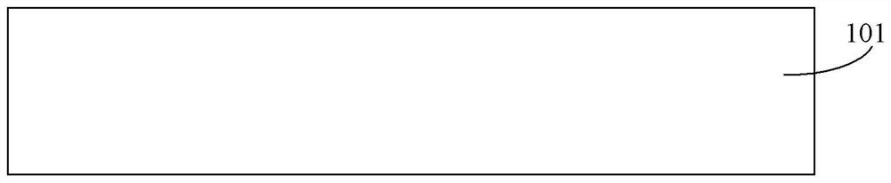
[0054] Step A1: If figure 1 As shown, a substrate 101 is provided.
[0055] Further, the substrate includes silicon, glass, quartz, and polymer; the substrate is not limited to the above four, and can be any substrate commonly used in microelectronics technology. The substrate can be a 4-inch, 6-inch, 8-inch, 12-inch wafer, and other substrates of different shapes and sizes suitable for micro-processing.
[0056] In this embodiment, a 4-inch monocrystalline silicon substrate is used.
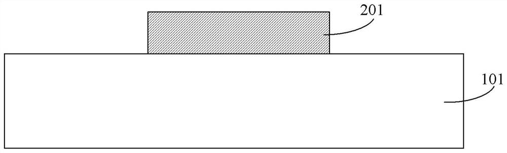
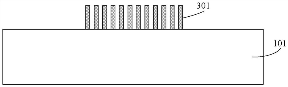
[0057] Step A2: forming a polymer layer 201 on the substrate 101 .
[0058] Further, the material of the polymer layer includes photoresist, polydimethylsiloxane, parylene, polyethylene, polycarbonate, and other polymer layers that can be removed by plasma bombardment Material;
[0059] The polymer layer can be disposed on the substrate 101 by means of spray coating, spin coating, p...
no. 3 example
[0106] The difference between the black silicon-based MEMS device preparation method provided in this embodiment and the second embodiment is that this embodiment uses a front-side release process to etch the substrate to form a back-side etching cavity for the MEMS sensor. The method includes the following steps:
[0107] Step C1 to step C3 are the same as step B1 to step B3.
[0108] Step C4: If Figure 13 As shown, a front corrosion release hole 501 is provided on the polymer layer, the sensor sensitive structure, and the sensor basic structure.
[0109] Further, the front corrosion release hole is prepared by photolithography or etching process, and the front corrosion release hole passes through the patterned polymer layer, the sensor sensitive structure and the sensor basic structure, and connects with the substrate 102 .
[0110] Step C5: If Figure 14 As shown, the substrate 102 is etched and released by front dry etching to form a back etching cavity 502 of the MEMS...
PUM
Property
Measurement
Unit
thickness
aaaaa
aaaaa
diameter
aaaaa
aaaaa
height
aaaaa
aaaaa
Abstract
The invention provides a black silicon preparation process. The preparation process comprises the steps of forming a polymer layer on a substrate; removing the polymer layer, and forming a nanometer forest structure at the initial position of the polymer layer by the product generated in the polymer layer removal process; and depositing a silicon thin film material layer on the nanometer forest structure to complete black silicon preparation. The invention also provides black silicon prepared by the black silicon preparation process, and a preparation method of a black silicon-based MEMS device. By virtue of the black silicon, the preparation process, and the preparation method of the black silicon-based MEMS device disclosed in the invention, the black silicon with higher optical absorption capability is prepared by the black silicon preparation process with low process cost and high popularity and adaptation; and in addition, by adoption of the preparation method of the black silicon-based MEMS device, corrosion damage to the black silicon in the releasing process of the MEMS device is avoided.
Description
technical field [0001] The disclosure belongs to the field of nanotechnology, and in particular relates to black silicon, a preparation process and a method for preparing a black silicon-based MEMS device. Background technique [0002] Black silicon is a forest-like large-area nano-column / needle structure, which was once considered a revolutionary new material in the electronics industry. Compared with traditional silicon materials, black silicon has extremely high absorption efficiency for light from visible to near-infrared. Various methods have been proposed to prepare black silicon, including high-energy femtosecond laser-assisted etching, metal-catalyzed electrochemical corrosion, and plasma dry etching. Due to the comprehensive consideration of processing cost, process convenience and process compatibility, the method of preparing black silicon by plasma dry etching technology is the most commonly used in conventional semiconductor processes, but this method may rely ...
Claims
Application Information
Patent Timeline
Application Date:The date an application was filed.
Publication Date:The date a patent or application was officially published.
First Publication Date:The earliest publication date of a patent with the same application number.
Issue Date:Publication date of the patent grant document.
PCT Entry Date:The Entry date of PCT National Phase.
Estimated Expiry Date:The statutory expiry date of a patent right according to the Patent Law, and it is the longest term of protection that the patent right can achieve without the termination of the patent right due to other reasons(Term extension factor has been taken into account ).
Invalid Date:Actual expiry date is based on effective date or publication date of legal transaction data of invalid patent.

