Eureka AIR delivers breakthrough ideas for toughest innovation challenges, trusted by R&D personnel around the world.

Processing method of PCB and PCB

A technology of processing method and slotting method, which is applied in the direction of electrical components, printed circuit manufacturing, printed circuit, etc., can solve the problems of irregular slot shape and difficulty in ensuring the quality of PCB production, etc.

Active Publication Date: 2018-03-20
MEIZHOU ZHIHAO ELECTRONICS TECH
View PDF2 Cites 5 Cited by
  • Summary
  • Abstract
  • Description
  • Claims
  • Application Information

AI Technical Summary

Problems solved by technology

[0003] At present, when the PCB needs to be slotted, the slot of the required shape is often directly drilled on the board surface. This slotting method is likely to cause irregular slot shapes, and it is difficult to ensure the production quality of the PCB.

Method used


Image

  • Processing method of PCB and PCB
  • Processing method of PCB and PCB
  • Processing method of PCB and PCB

Examples


Embodiment Construction

[0033] In order to make the purpose, features and advantages of the present invention more obvious and understandable, the technical solutions in the embodiments of the present invention will be clearly and completely described below in conjunction with the accompanying drawings in the embodiments of the present invention. Obviously, the following The described embodiments are only some, not all, embodiments of the present invention. Based on the embodiments of the present invention, all other embodiments obtained by persons of ordinary skill in the art without making creative efforts belong to the protection scope of the present invention.

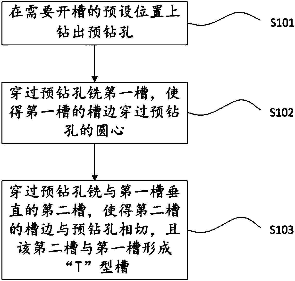
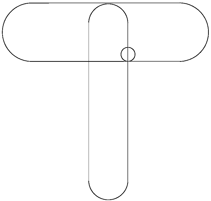
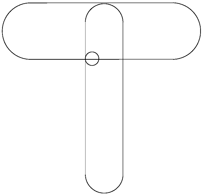
[0034] see figure 1 , figure 1 The process flow of the PCB processing method is shown.

[0035] In the present embodiment, the processing method of PCB comprises the following steps:

[0036] S101. Drill a pre-drilled hole at a preset position to be slotted.

[0037] In this step, the specific manufacturing process is:

[0038] 1) Se...


PUM


Abstract

The present invention discloses a processing method of a PCB (Printed Circuit Board) and a PCB. The processing method comprises the steps of: drilling a prebored hole on a board; passing through the prebored hole to mill a first groove, wherein a groove edge of the first groove passes through the center of a circle of the prebored hole; and passing through the prebored hole to mill a second groovebeing perpendicular to the first groove, wherein a groove edge of the second groove is tangent to the prebored hole, and the second groove and the first groove form a T-shaped groove. The prebored hole is drilled in advance to determine the grooving positions and directions of the first groove and the second groove, and therefore, the manufactured T-shaped groove shape rule is ensured to satisfythe production demand.

Description

technical field [0001] The invention relates to the technical field of PCBs, in particular to a PCB processing method and the PCB. Background technique [0002] PCB (Printed Circuit Board), the Chinese name is printed circuit board, also known as printed circuit board, is an important electronic component, a support for electronic components, and a carrier for electrical connections of electronic components. When assembling and assembling PCBs, it is often necessary to slot on the PCB. [0003] At present, when the PCB needs to be slotted, the slots of the required shape are often directly drilled on the board surface. This slotting method easily leads to irregular slot shapes, and it is difficult to ensure the production quality of the PCB. Contents of the invention [0004] The object of the present invention is to provide a PCB processing method and PCB, which can overcome the groove shape irregularity that occurs when making "T-shaped grooves" on PCBs in the prior art...

Claims


Application Information

Patent Timeline
Patent Type & Authority Applications(China)
IPC IPC(8): H05K3/00
CPCH05K3/0044H05K2203/0271
Inventor 张学平刘喜科戴晖
Owner MEIZHOU ZHIHAO ELECTRONICS TECH
Why Eureka
Eureka Blog
Learn More