Impedance matching circuit board, antenna and terminal

An impedance matching circuit and impedance matching technology, applied in the radio frequency field, can solve high cost problems, achieve the effect of solving high cost problems, improving dispersion and reliability

Inactive Publication Date: 2018-04-03
YULONG COMPUTER TELECOMM SCI (SHENZHEN) CO LTD
View PDF4 Cites 10 Cited by
  • Summary
  • Abstract
  • Description
  • Claims
  • Application Information

AI Technical Summary

Problems solved by technology

[0006] The present invention is based on at least one of the above-mentioned technical problems, and proposes a new impedance matching circuit board, which improves the discreteness of the radio frequency circuit by setting the microstrip line (or called a stub line) in the lumped element circuit. High degree and reliability, solving the high cost problem of lumped elements with small reactance values

Method used


Image

  • Impedance matching circuit board, antenna and terminal
  • Impedance matching circuit board, antenna and terminal
  • Impedance matching circuit board, antenna and terminal

Examples


Embodiment 1

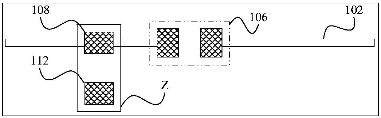
[0073] Such as Figure 4 with Figure 5 As shown, preferably, a first resistor or a first inductor or a first capacitor 116A (welding area 116) is welded between the first pad 110 and the common pad 108, the second pad 112 is unloaded, and the lumped element circuit It also includes: a third pad 114 disposed on a side of the first pad 110 away from the common pad 108 , and a microstrip line 104 is welded between the first pad 110 and the third pad 114 .

Embodiment 2

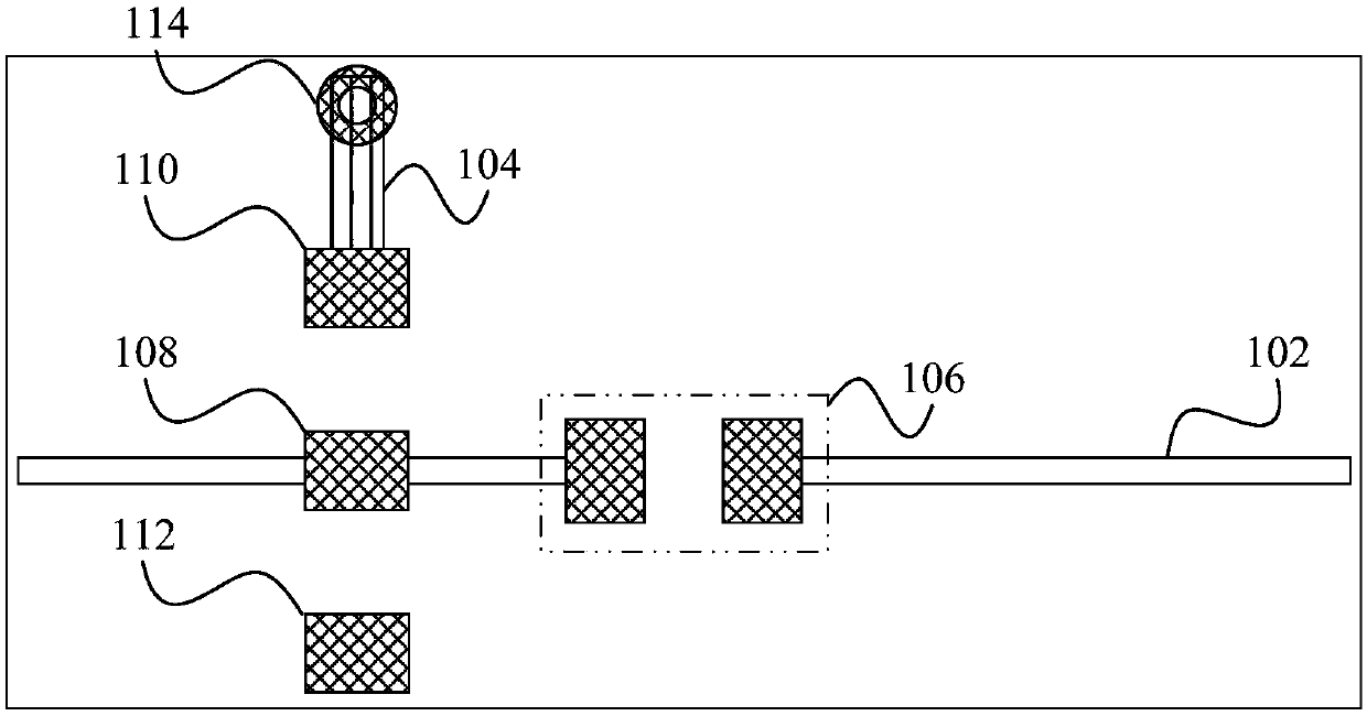
[0075] Such as Figure 4 with Image 6 As shown, preferably, a second resistor or a second inductance or a second capacitor 118A (welding area 118) is welded between the second pad 112 and the common pad 108, and the lumped element circuit also includes: a third pad 114 , located on the side of the first pad 110 away from the common pad 108 , and the microstrip line 104 is welded between the first pad 110 and the third pad 114 .

Embodiment 3

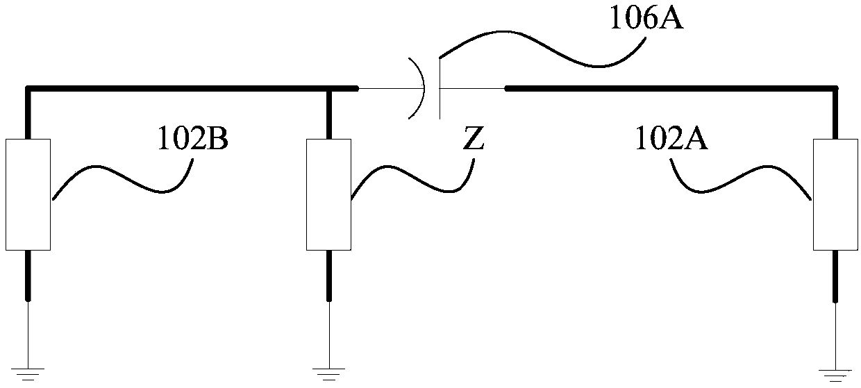
[0077] Such as Figure 7 As shown, the L-shaped filter circuit includes a parallel connection of a first inductor L11, a second inductor L12, equivalent resistances 102A and 102B of transmission lines, a capacitor 106A is used to filter DC interference, and a microstrip line 104 is short-circuited to the second inductor L12.

[0078] Such as Figure 8 As shown, the L-shaped filter circuit includes a parallel connection of a first capacitor C11, a second capacitor C12, and equivalent resistances 102A and 102B of the transmission line. The capacitor 106A is used to filter DC interference, and the microstrip line 104 is short-circuited to the second inductor C12.

[0079] Such as Figure 4 to Figure 9 As shown, preferably, a first resistor or a first inductance or a first capacitor 116A (welding area 116) is welded between the first pad 110 and the common pad 108, and between the second pad 112 and the common pad 108 A second resistance or a second inductance or a second capaci...


PUM


Abstract

The invention provides an impedance matching circuit board, an antenna and a terminal. The impedance matching circuit board comprises a microstrip line. The microstrip line is in short circuit connection with an assigned member in a lumped element circuit or is in an open circuit connection with the periphery of the assigned member for performing impedance matching with the assigned member. The impedance value of the microstrip line is determined by a working frequency of an electromagnetic signal. A common welding plate is arranged in the lumped element circuit and the common welding plate isused for welding pins of multiple assigned members. The impedance matching circuit board, the antenna and the terminal improve a matching degree of the impedance circuit and element discretness.

Description

technical field [0001] The present invention relates to the field of radio frequency technology, in particular to an impedance matching circuit board, an antenna and a terminal. Background technique [0002] In the related technology of radio frequency circuit, L-shaped filter circuit as a mainstream impedance matching circuit includes more than two lumped elements. Common lumped elements include capacitors, inductors and resistors. The reactance value is discontinuous, such as the inductance value is 0.6nH, 0.9nH, 1nH, 1.2nH, 1.3nH, 1.5nH, 1.8nH, 2nH, 2.2nH, 2.4nH, 2.7nH, 2.9nH, 3nH, 3.3nH ... 18nH, 27nH, 33nH... . [0003] Impedance matching based on common lumped elements has at least the following technical defects: [0004] (1) Because the reactance value of the lumped element is relatively discrete, RF engineers are concerned about the process cost. For example, it is difficult to achieve accurate impedance matching if there is no inductance less than 0.6nH; [0005...

Claims


Application Information

Patent Timeline
Patent Type & Authority Applications(China)
IPC IPC(8): H05K1/02H05K1/18H01Q1/38H01Q13/08
CPCH01Q1/38H01Q13/08H05K1/025H05K1/18H05K1/02
Inventor 信哲鑫
Owner YULONG COMPUTER TELECOMM SCI (SHENZHEN) CO LTD
Why Eureka
Try Eureka