Coating micro-drilling knife for printed circuit board machining and preparation method thereof

A printed circuit board and micro-drilling technology, which is applied in coating, metal processing, metal material coating technology, etc., can solve the problems that cannot meet the service conditions of high-speed cutting, and achieve simple operability, good adhesion, Effect of Low Coefficient of Friction

Inactive Publication Date: 2018-04-06
ZHOUKOU NORMAL UNIV
View PDF10 Cites 3 Cited by
  • Summary
  • Abstract
  • Description
  • Claims
  • Application Information

AI Technical Summary

Problems solved by technology

[0007] Nitride-based nano-multilayer coatings such as TiN coatings have a hardness of HV25±2GPa and an oxidation temperature of about 500°C; TiCN coatings have a hardness as high as HV40 but an oxidation resistance temper

Method used


Image

  • Coating micro-drilling knife for printed circuit board machining and preparation method thereof

Examples


Embodiment 1

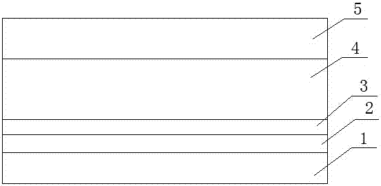
[0028] Such as figure 1 As shown, a coated micro-drill for processing printed circuit boards includes a micro-drill substrate 1, and the micro-drill substrate 1 is sequentially attached with a metallurgical bonding layer 2, a transition layer 3, and a main resistance layer from the inside to the outside. The grinding layer 4 and the self-lubricating layer 5, the metallurgical bonding layer 2 is a pure metal Cr layer, the transition layer 3 is a nano-multilayer composed of Cr and VN alternately, and the main wear-resistant layer 4 is a nano-multilayer composed of DLC and VN alternately. The lubricating layer 5 is a Cr-doped DLC layer.

[0029] The thickness of the transition layer 3 is 100-200 nm, the thickness of the main wear-resistant layer 4 is 500-1500 nm, and the thickness of the self-lubricating layer 5 is 200-500 nm.

[0030] In the transition layer 3, the thickness of a single layer of Cr is 10-20 nm, and the thickness of a single layer of VN is 5-15 nm.

[0031] In ...

Embodiment 2

[0043] A coated micro-drill for processing printed circuit boards, comprising a micro-drill substrate, on which a metallurgical bonding layer, a transition layer, a main wear-resistant layer and a self-lubricating layer are sequentially attached from the inside to the outside, The metallurgical bonding layer is a pure metal Cr layer, the transition layer is a nano-multilayer composed of Cr and VN alternately, the main wear-resistant layer is a nano-multilayer composed of DLC and VN alternately, and the self-lubricating layer is a Cr-doped DLC layer.

[0044] The thickness of the transition layer is 100nm, the thickness of the main wear-resistant layer is 500nm, and the thickness of the self-lubricating layer is 200nm. In the transition layer, the single-layer Cr thickness is 10nm, and the single-layer VN thickness is 8nm. In the main wear-resistant layer, the single-layer DLC has a thickness of 5nm, and the single-layer VN has a thickness of 10nm.

[0045] The material of the...

Embodiment 3

[0055] A coated micro-drill for processing printed circuit boards, comprising a micro-drill substrate, on which a metallurgical bonding layer, a transition layer, a main wear-resistant layer and a self-lubricating layer are sequentially attached from the inside to the outside, The metallurgical bonding layer is a pure metal Cr layer, the transition layer is a nano-multilayer composed of Cr and VN alternately, the main wear-resistant layer is a nano-multilayer composed of DLC and VN alternately, and the self-lubricating layer is a Cr-doped DLC layer.

[0056] The thickness of the transition layer is 120nm, the thickness of the main wear-resistant layer is 600nm, and the thickness of the self-lubricating layer is 300nm. In the transition layer, the single-layer Cr thickness is 12nm, and the single-layer VN thickness is 6nm. In the main wear-resistant layer, the single-layer DLC has a thickness of 6nm, and the single-layer VN has a thickness of 9nm.

[0057] The material of the ...


PUM

PropertyMeasurementUnit
Thicknessaaaaaaaaaa
Thicknessaaaaaaaaaa
Thicknessaaaaaaaaaa

Abstract

The invention discloses a coating micro-drilling knife for printed circuit board machining. The coating micro-drilling knife comprises a micro-drilling knife base body, wherein a metallurgical bondinglayer, a transition layer, a main wear-resistant layer and a self-lubricating layer are sequentially attached to the micro-drilling knife base body from inside to outside; and the metallurgical bonding layer is a pure metal Cr layer, the transition layer is a nano multilayer formed by alternating Cr and Vn, the main wear-resistant layer is a nano multilayer formed by alternating DLC and VN, and the self-lubricating layer is a Cr-doped DLC layer. According to the coating structure, on one hand, the composite coating has relatively high performance; and on the other hand, the coating and the base body can have good adhesive force; and meanwhile, operability is simple and feasible. The coating micro-drilling knife has good film-base binding force, high hardness (greater than 20 GPa) and lowfriction coefficient (less than 0.3).

Description

technical field [0001] The invention provides a coated micro-drill for processing printed circuit boards and a preparation method thereof, which is applied to the processing and manufacturing of printed circuit boards and can also be used for drilling of thin metal plates, and belongs to the field of mechanical processing and manufacturing. Background technique [0002] Printed circuit board (PCB-Printed Circuit Board) is an indispensable basic component of all electronic information products, and it is also the product with the highest market share in the global electronic component products. The miniaturization of components mounted on the printed circuit board (PCB) of mobile phones, notebook computers and other products not only promotes the development of miniaturization of printed circuit boards, but also promotes the fine circuit patterns of printed circuit boards. . [0003] Vias are one of the important components of PCB, and their functions are the electrical conn...

Claims


Application Information

Patent Timeline
IPC IPC(8): C23C14/06C23C14/16C23C14/18C23C14/35B26D1/00B26F1/16
CPCB26D1/0006B26D2001/002B26F1/16B26F2210/08C23C14/0605C23C14/0641C23C14/165C23C14/185C23C14/345C23C14/35
Inventor 周小东张松锋王永梅谷雨周思华周小宇
Owner ZHOUKOU NORMAL UNIV
Why Eureka
Try Eureka